- 您現(xiàn)在的位置:買賣IC網(wǎng) > PDF目錄9995 > IDT72825LB15PF (IDT, Integrated Device Technology Inc)IC FIFO SYNC DL 1024X18 128TQFP PDF資料下載
參數(shù)資料
| 型號: | IDT72825LB15PF |
| 廠商: | IDT, Integrated Device Technology Inc |
| 文件頁數(shù): | 12/26頁 |
| 文件大?。?/td> | 0K |
| 描述: | IC FIFO SYNC DL 1024X18 128TQFP |
| 標準包裝: | 72 |
| 系列: | 7200 |
| 功能: | 同步 |
| 存儲容量: | 18.4K(1K x 18) |
| 數(shù)據(jù)速率: | 67MHz |
| 訪問時間: | 15ns |
| 電源電壓: | 4.5 V ~ 5.5 V |
| 工作溫度: | 0°C ~ 70°C |
| 安裝類型: | 表面貼裝 |
| 封裝/外殼: | 128-LQFP |
| 供應商設(shè)備封裝: | 128-TQFP(14x20) |
| 包裝: | 托盤 |
| 其它名稱: | 72825LB15PF |

COMMERCIALANDINDUSTRIAL
TEMPERATURERANGES
IDT72805LB/72815LB/72825LB/72835LB/72845LB CMOS Dual SyncFIFOTM
256 x 18, 512 x 18, 1,024 x 18, 2,048 x 18 and 4,096 x 18
2
JANUARY 13, 2009
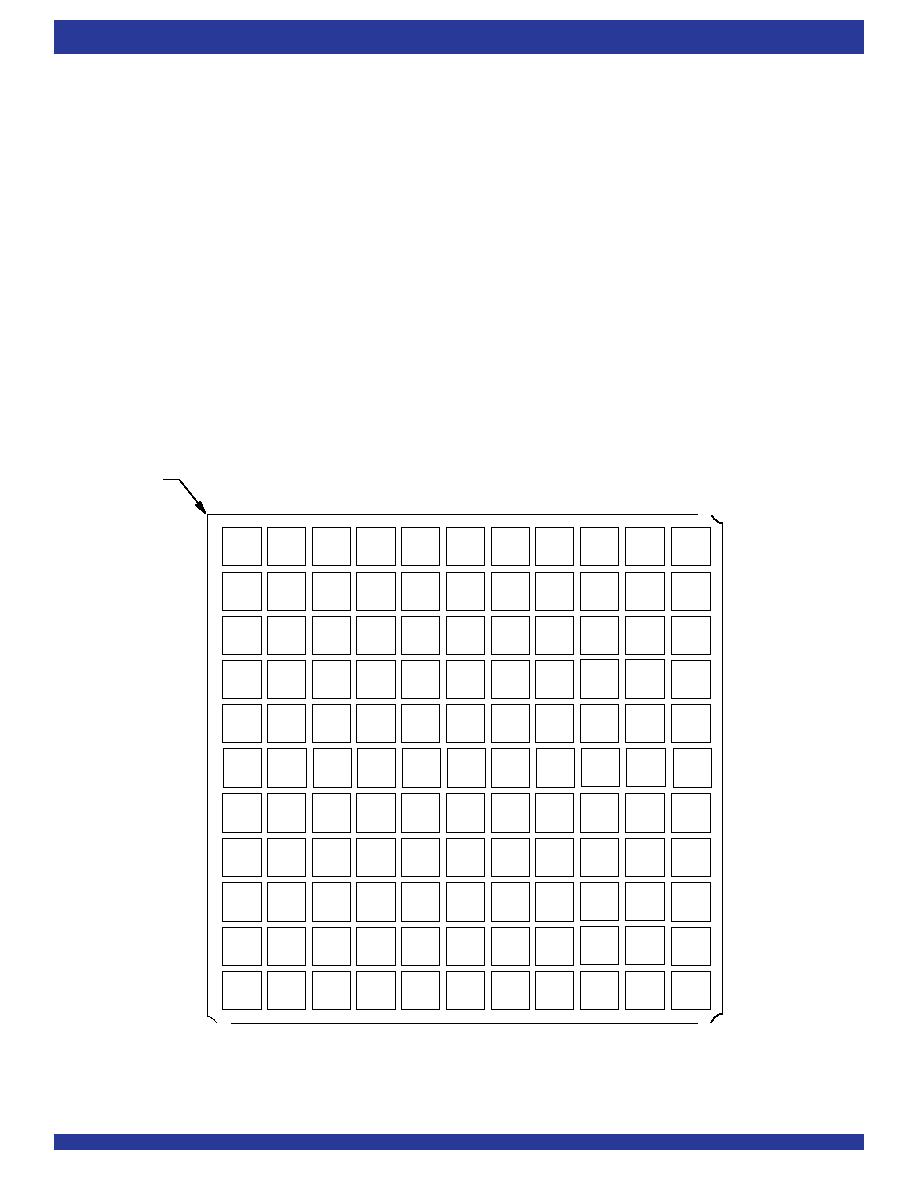
PIN CONFIGURATIONS
WCLKA
DA3
DA1
DA0
DB13
DB16
RCLKB
LDB
RSB
QB17
QB16
PAFA
DA4
WENA
DA2
DB12
DB15
RENB
OEB
EFB
QB15
QB14
FFA
RXIA
WXIA
DA5
DB14
DB11
GND
DB17
GND
QB13
QB11
QB8
QB10
QB12
VCC
DB7
DB10
DB8
FLA
QA2
QA0
RXOA
QA1
QA4
QA3
WXOA/
HFA
PAEA
DB9
DB6
VCC
QB9
QB7
QA5
QA6
GND
VCC
GND
VCC
GND
QB6
QB5
QA7
QA9
VCC
DA6
DA9
PAEB
WXOB/
HFB
QB3
QB4
QB1
QA8
QA10
QA12
VCC
DA7
DA10
DA8
FLB
QB2
QB0
RXOB
QA11
QA13
GND
DA17
GND
DA11
DA14
DB5
WXIB
RXIB
FFB
QA14
QA15
EFA
OEA
RENA
DA15
DA12
DB2
WENB
DB4
PAFB
QA16
QA17
RSA
LDA
RCKLA
DA16
DA13
DB0
DB1
DB3
WCLKB
123
456
789
10
11
A
B
C
D
E
F
G
H
J
K
L
PIN 1
3139 drw 02
PBGA (BG121-1, order code: BG)
TOP VIEW
NOTE:
1.
The PBGA is only available for the IDT72805LB/72815LB/72825LB in the 15 or 25 ns speed grade.
72815LB/72825LB/72835LB/72845LB device is functionally equivalent to two
IDT72205LB/72215LB/72225LB/72235LB/72245LB FIFOs in a single pack-
agewithallassociatedcontrol,data,andflaglinesassignedtoindependentpins.
These devices are very high-speed, low-power First-In, First-Out (FIFO)
memorieswithclockedreadandwritecontrols.TheseFIFOsareapplicablefor
awidevarietyofdatabufferingneeds,suchasopticaldiskcontrollers,LocalArea
Networks(LANs),andinterprocessorcommunication.
Each of the two FIFOs contained in these devices has an 18-bit input and
output port. Each input port is controlled by a free-running clock (WCLK), and
an input enable pin (
WEN). Data is read into the synchronous FIFO on every
clock when
WEN is asserted. The output port of each FIFO bank is controlled
by another clock pin (RCLK) and another enable pin (
REN). The Read Clock
can be tied to the Write Clock for single clock operation or the two clocks can
run asynchronous of one another for dual-clock operation. An Output Enable
pin (
OE) is provided on the read port of each FIFO for three-state control of the
output.
The synchronous FIFOs have two fixed flags, Empty Flag/Output Ready
(
EF/OR) and Full Flag/Input Ready (FF/IR), and two programmable flags,
Almost-Empty(
PAE)andAlmost-Full(PAF).Theoffsetloadingoftheprogram-
mable flags is controlled by a simple state machine, and is initiated by asserting
the Load pin (
LD). A Half-Full flag (HF) is available for each FIFO that is
implemented as a single device configuration.
There are two possible timing modes of operation with these devices: IDT
Standard mode and First Word Fall Through (FWFT) mode.
In IDT Standard Mode, the first word written to an empty FIFO will not
appear on the data output lines unless a specific read operation is performed.
A read operation, which consists of activating
REN and enabling a rising RCLK
edge, will shift the word from internal memory to the data output lines.
In FWFT mode, the first word written to an empty FIFO is clocked directly
to the data output lines after three transitions of the RCLK signal. A
REN does
not have to be asserted for accessing the first word.
These devices are depth expandable using a daisy-chain technique or First
Word Fall Through (FWFT) mode. The
XI and XO pins are used to expand the
FIFOs. In depth expansion configuration,
FLisgroundedonthefirstdeviceand
set to HIGH for all other devices in the Daisy Chain.
The IDT72805LB/72815LB/72825LB/72835LB/72845LB are fabricated
using IDT’s high-speed submicron CMOS technology.
DESCRIPTION (Continued)
相關(guān)PDF資料 |
PDF描述 |
|---|---|
| MS27472T12F35P | CONN RCPT 22POS WALL MNT W/PINS |
| IDT72V3650L6PFG8 | IC FIFO SS 2048X36 6NS 128-TQFP |
| MS3100A28-2P | CONN RCPT 14POS WALL MNT W/PINS |
| MS27473E10F35SA | CONN PLUG 13POS STRAIGHT W/SCKT |
| MS27497T8F35PA | CONN RCPT 6POS WALL MNT W/PINS |
相關(guān)代理商/技術(shù)參數(shù) |
參數(shù)描述 |
|---|---|
| IDT72825LB15PF8 | 功能描述:IC FIFO SYNC DL 1024X18 128TQFP RoHS:否 類別:集成電路 (IC) >> 邏輯 - FIFO 系列:7200 標準包裝:90 系列:7200 功能:同步 存儲容量:288K(16K x 18) 數(shù)據(jù)速率:100MHz 訪問時間:10ns 電源電壓:4.5 V ~ 5.5 V 工作溫度:0°C ~ 70°C 安裝類型:表面貼裝 封裝/外殼:64-LQFP 供應商設(shè)備封裝:64-TQFP(14x14) 包裝:托盤 其它名稱:72271LA10PF |
| IDT72825LB15PFGI | 制造商:Integrated Device Technology Inc 功能描述:IC FIFO SYNC DL 1024X18 128TQFP |
| IDT72825LB15PFGI8 | 制造商:Integrated Device Technology Inc 功能描述:IC FIFO SYNC DL 1024X18 128TQFP |
| IDT72825LB15PFI | 功能描述:IC FIFO SYNC DL 1024X18 128TQFP RoHS:否 類別:集成電路 (IC) >> 邏輯 - FIFO 系列:7200 標準包裝:90 系列:7200 功能:同步 存儲容量:288K(16K x 18) 數(shù)據(jù)速率:100MHz 訪問時間:10ns 電源電壓:4.5 V ~ 5.5 V 工作溫度:0°C ~ 70°C 安裝類型:表面貼裝 封裝/外殼:64-LQFP 供應商設(shè)備封裝:64-TQFP(14x14) 包裝:托盤 其它名稱:72271LA10PF |
| IDT72825LB15PFI8 | 功能描述:IC FIFO SYNC DL 1024X18 128TQFP RoHS:否 類別:集成電路 (IC) >> 邏輯 - FIFO 系列:7200 標準包裝:90 系列:7200 功能:同步 存儲容量:288K(16K x 18) 數(shù)據(jù)速率:100MHz 訪問時間:10ns 電源電壓:4.5 V ~ 5.5 V 工作溫度:0°C ~ 70°C 安裝類型:表面貼裝 封裝/外殼:64-LQFP 供應商設(shè)備封裝:64-TQFP(14x14) 包裝:托盤 其它名稱:72271LA10PF |
發(fā)布緊急采購,3分鐘左右您將得到回復。