- 您現(xiàn)在的位置:買賣IC網(wǎng) > PDF目錄377522 > IRHNA54160 (International Rectifier) Surface Mount Radiation Hardened Power MOSFET(表貼型抗輻射功率MOS場(chǎng)效應(yīng)管) PDF資料下載
參數(shù)資料
| 型號(hào): | IRHNA54160 |
| 廠商: | International Rectifier |
| 英文描述: | Surface Mount Radiation Hardened Power MOSFET(表貼型抗輻射功率MOS場(chǎng)效應(yīng)管) |
| 中文描述: | 表面安裝抗輻射功率MOSFET(表貼型抗輻射功率馬鞍山場(chǎng)效應(yīng)管) |
| 文件頁(yè)數(shù): | 2/8頁(yè) |
| 文件大?。?/td> | 101K |
| 代理商: | IRHNA54160 |
IRHNA57160
Pre-Irradiation
2
www.irf.com
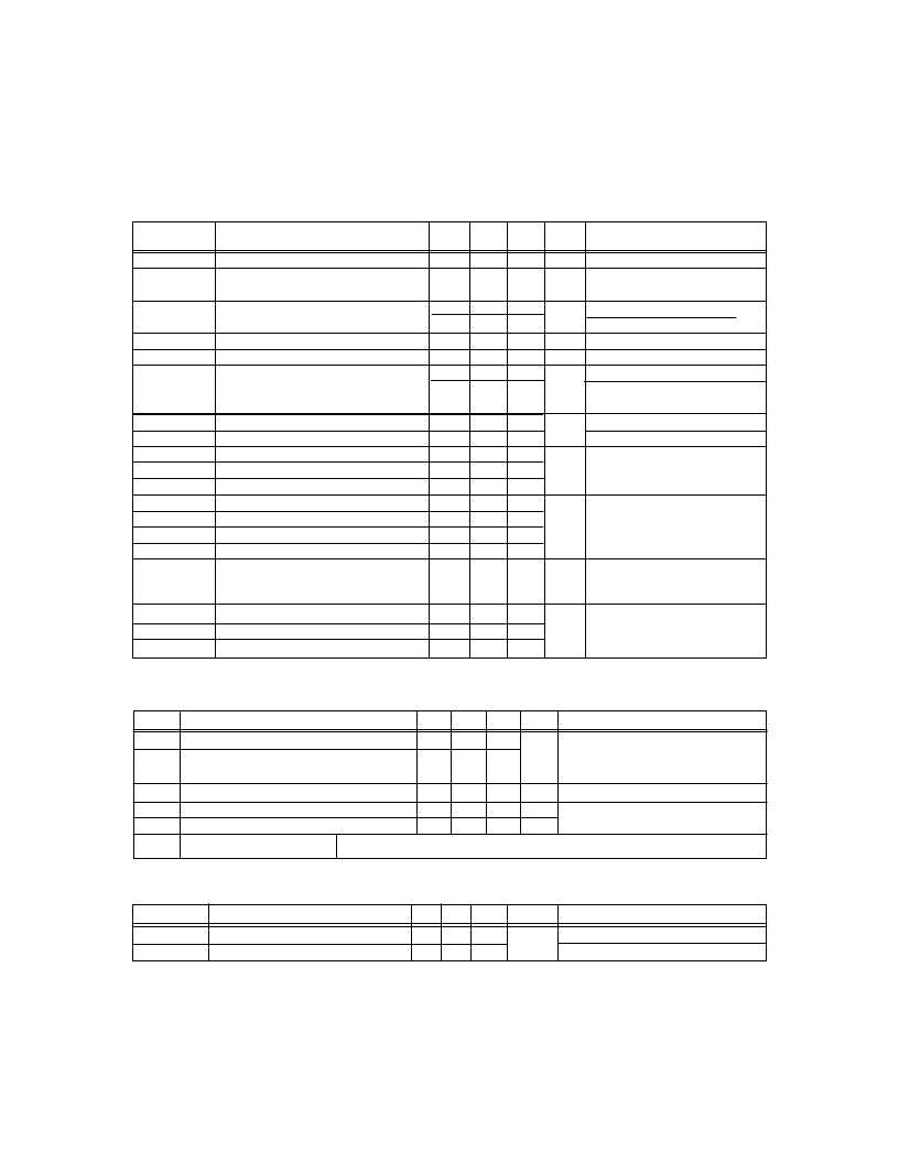
Electrical Characteristics
@ Tj = 25°C (Unless Otherwise Specified)
Parameter
Drain-to-Source Breakdown Voltage
BVDSS/
TJ Temperature Coefficient of Breakdown
Voltage
RDS(on)
Static Drain-to-Source On-State
Resistance
VGS(th)
Gate Threshold Voltage
gfs
Forward Transconductance
IDSS
Zero Gate Voltage Drain Current
Min
100
—
Typ
—
0.115
Max Units
—
—
Test Conditions
VGS = 0V, ID = 1.0mA
Reference to 25°C, ID = 1.0mA
BVDSS
V
V/°C
—
—
2.0
42
—
—
—
—
—
—
—
—
0.013
0.012
4.0
—
10
25
VGS = 12V, ID = 75A
VGS = 12V, ID = 69A
VDS = VGS, ID = 1.0mA
VDS > 15V, IDS = 69A
VDS= 80V ,VGS=0V
VDS = 80V,
VGS = 0V, TJ = 125°C
VGS = 20V
VGS = -20V
VGS =12V, ID = 75A
VDS = 50V
V
S (
)
IGSS
IGSS
Qg
Qgs
Qgd
td
(on)
tr
td
(off)
tf
LS + LD
Gate-to-Source Leakage Forward
Gate-to-Source Leakage Reverse
Total Gate Charge
Gate-to-Source Charge
Gate-to-Drain (‘Miller’) Charge
Turn-On Delay Time
Rise Time
Turn-Off Delay Time
Fall Time
Total Inductance
—
—
—
—
—
—
—
—
—
—
—
—
—
—
—
—
—
—
—
4.0
100
-100
160
55
65
35
125
75
50
—
nC
VDD = 50V, ID = 75A,
RG = 2.35
Ciss
Coss
Crss
Input Capacitance
Output Capacitance
Reverse Transfer Capacitance
—
—
—
6440
1660
60
—
—
—
VGS = 0V, VDS = 25V
f = 1.0MHz
pF
nA
nH
ns
μ
A
Thermal Resistance
Parameter
RthJC
Junction-to-Case
RthJ-PCB
Junction-to-PC board
Min Typ Max
—
—
—
1.6
Units
Test Conditions
0.42
—
soldered to a 2” square copper-clad board
°C/W
Measured from the center of
drain pad to center of source pad
Note: Corresponding Spice and Saber models are available on the G&S Website.
For footnotes refer to the last page
Source-Drain Diode Ratings and Characteristics
Parameter
IS
Continuous Source Current (Body Diode)
ISM
Pulse Source Current (Body Diode)
Min Typ
—
—
Max Units
75*
300
Test Conditions
—
—
VSD
trr
QRR
ton
Diode Forward Voltage
Reverse Recovery Time
Reverse Recovery Charge
—
—
—
—
—
—
1.2
300
2.2
V
nS
μ
C
T
j
= 25°C, IS = 75A, VGS = 0V
Tj = 25°C, IF = 35A, di/dt
≥
100A/
μ
s
VDD
≤
25V
Forward Turn-On Time
Intrinsic turn-on time is negligible. Turn-on speed is substantially controlled by LS + LD.
A
* Current is limited by internal wire diameter
相關(guān)PDF資料 |
PDF描述 |
|---|---|
| IRHNA53260 | 200V, N-CHANNEL |
| IRHNA57060 | 200V, N-CHANNEL |
| IRHNA54260 | 200V, N-CHANNEL |
| IRHNA57260 | 200V, N-CHANNEL |
| IRHNA58260 | 200V, N-CHANNEL |
相關(guān)代理商/技術(shù)參數(shù) |
參數(shù)描述 |
|---|---|
| IRHNA54260 | 制造商:International Rectifier 功能描述:HIREL, HEXFET RHD - Bulk |
| IRHNA54Z60 | 制造商:International Rectifier 功能描述:MOSFET, HIREL, RAD HARD, R5 - Bulk |
| IRHNA57060 | 制造商:IRF 制造商全稱:International Rectifier 功能描述:200V, N-CHANNEL |
| IRHNA57064 | 制造商:IRF 制造商全稱:International Rectifier 功能描述:RADIATION HARDENED POWER MOSFET SURFACE MOUNT (SMD-2) |
| IRHNA57064/SLDC/BAE | 制造商:International Rectifier 功能描述:TRANS MOSFET N-CH 60V 75A 3SMD-2 SLDC FOR BAE - Virtual or Non-Physical Inventory (Software & Literature) |
發(fā)布緊急采購(gòu),3分鐘左右您將得到回復(fù)。