- 您現(xiàn)在的位置:買賣IC網(wǎng) > PDF目錄45377 > IS80C52CXXX-36:R (TEMIC SEMICONDUCTORS) 8-BIT, MROM, 36 MHz, MICROCONTROLLER, PQCC44 PDF資料下載
參數(shù)資料
| 型號(hào): | IS80C52CXXX-36:R |
| 廠商: | TEMIC SEMICONDUCTORS |
| 元件分類: | 微控制器/微處理器 |
| 英文描述: | 8-BIT, MROM, 36 MHz, MICROCONTROLLER, PQCC44 |
| 文件頁數(shù): | 66/344頁 |
| 文件大小: | 4745K |
第1頁第2頁第3頁第4頁第5頁第6頁第7頁第8頁第9頁第10頁第11頁第12頁第13頁第14頁第15頁第16頁第17頁第18頁第19頁第20頁第21頁第22頁第23頁第24頁第25頁第26頁第27頁第28頁第29頁第30頁第31頁第32頁第33頁第34頁第35頁第36頁第37頁第38頁第39頁第40頁第41頁第42頁第43頁第44頁第45頁第46頁第47頁第48頁第49頁第50頁第51頁第52頁第53頁第54頁第55頁第56頁第57頁第58頁第59頁第60頁第61頁第62頁第63頁第64頁第65頁當(dāng)前第66頁第67頁第68頁第69頁第70頁第71頁第72頁第73頁第74頁第75頁第76頁第77頁第78頁第79頁第80頁第81頁第82頁第83頁第84頁第85頁第86頁第87頁第88頁第89頁第90頁第91頁第92頁第93頁第94頁第95頁第96頁第97頁第98頁第99頁第100頁第101頁第102頁第103頁第104頁第105頁第106頁第107頁第108頁第109頁第110頁第111頁第112頁第113頁第114頁第115頁第116頁第117頁第118頁第119頁第120頁第121頁第122頁第123頁第124頁第125頁第126頁第127頁第128頁第129頁第130頁第131頁第132頁第133頁第134頁第135頁第136頁第137頁第138頁第139頁第140頁第141頁第142頁第143頁第144頁第145頁第146頁第147頁第148頁第149頁第150頁第151頁第152頁第153頁第154頁第155頁第156頁第157頁第158頁第159頁第160頁第161頁第162頁第163頁第164頁第165頁第166頁第167頁第168頁第169頁第170頁第171頁第172頁第173頁第174頁第175頁第176頁第177頁第178頁第179頁第180頁第181頁第182頁第183頁第184頁第185頁第186頁第187頁第188頁第189頁第190頁第191頁第192頁第193頁第194頁第195頁第196頁第197頁第198頁第199頁第200頁第201頁第202頁第203頁第204頁第205頁第206頁第207頁第208頁第209頁第210頁第211頁第212頁第213頁第214頁第215頁第216頁第217頁第218頁第219頁第220頁第221頁第222頁第223頁第224頁第225頁第226頁第227頁第228頁第229頁第230頁第231頁第232頁第233頁第234頁第235頁第236頁第237頁第238頁第239頁第240頁第241頁第242頁第243頁第244頁第245頁第246頁第247頁第248頁第249頁第250頁第251頁第252頁第253頁第254頁第255頁第256頁第257頁第258頁第259頁第260頁第261頁第262頁第263頁第264頁第265頁第266頁第267頁第268頁第269頁第270頁第271頁第272頁第273頁第274頁第275頁第276頁第277頁第278頁第279頁第280頁第281頁第282頁第283頁第284頁第285頁第286頁第287頁第288頁第289頁第290頁第291頁第292頁第293頁第294頁第295頁第296頁第297頁第298頁第299頁第300頁第301頁第302頁第303頁第304頁第305頁第306頁第307頁第308頁第309頁第310頁第311頁第312頁第313頁第314頁第315頁第316頁第317頁第318頁第319頁第320頁第321頁第322頁第323頁第324頁第325頁第326頁第327頁第328頁第329頁第330頁第331頁第332頁第333頁第334頁第335頁第336頁第337頁第338頁第339頁第340頁第341頁第342頁第343頁第344頁
158
AT90PWM216/316 [DATASHEET]
7710H–AVR–07/2013
When set, this bit prevails over PARUN0 bit.
15.25.12 PSC 1 Control Register – PCTL1
Bit 7:6 – PPRE11:0 : PSC 1 Prescaler Select
This two bits select the PSC input clock division factor.All generated waveform will be modified by this factor.
Bit 5 – PBFM1 : Balance Flank Width Modulation
When this bit is clear, Flank Width Modulation operates on On-Time 1 only.
When this bit is set, Flank Width Modulation operates on On-Time 0 and On-Time 1.
Bit 4 – PAOC1B : PSC 1 Asynchronous Output Control B
When this bit is set, Fault input selected to block B can act directly to PSCOUT11 output. See “PSC Input Configu-
Bit 3 – PAOC1A : PSC 1 Asynchronous Output Control A
When this bit is set, Fault input selected to block A can act directly to PSCOUT10 output. See “PSC Input Configu-
Bit 2 – PARUN1 : PSC 1 Autorun
When this bit is set, the PSC 1 starts with PSC0. That means that PSC 1 starts :
when PRUN0 bit in PCTL0 register is set,
or when PARUN0 bit in PCTL0 is set and PRUN2 bit in PCTL2 register is set.
Thanks to this bit, 2 or 3 PSCs can be synchronized (motor control for example)
Bit 1 – PCCYC1 : PSC 1 Complete Cycle
When this bit is set, the PSC 1 completes the entire waveform cycle before halt operation requested by clearing
PRUN1. This bit is not relevant in slave mode (PARUN1 = 1).
Bit 0 – PRUN1 : PSC 1 Run
Writing this bit to one starts the PSC 1.
When set, this bit prevails over PARUN1 bit.
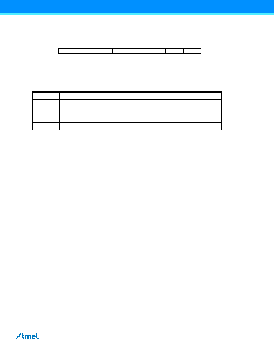
Bit
7
654
3
2
1
0
PPRE11
PPRE10
PBFM1
PAOC1B
PAOC1A
PARUN1
PCCYC1
PRUN1
PCTL1
Read/Write
R/W
Initial Value
0
Table 15-15. PSC 1 Prescaler Selection
PPRE11
PPRE10
Description
0
No divider on PSC input clock
0
1
Divide the PSC input clock by 4
1
0
Divide the PSC input clock by 32
1
Divide the PSC clock by 256
相關(guān)PDF資料 |
PDF描述 |
|---|---|
| MR83C154TXXX-12/883R | 8-BIT, MROM, 12 MHz, MICROCONTROLLER, CQCC44 |
| MD80C52XXX-12SBD | 8-BIT, MROM, 12 MHz, MICROCONTROLLER, CDIP40 |
| MR80C52TXXX-12SBR | 8-BIT, MROM, 12 MHz, MICROCONTROLLER, CQCC44 |
| MR80C52EXXX-16SC | 8-BIT, MROM, 16 MHz, MICROCONTROLLER, CQCC44 |
| MQ80C32-20P883D | 8-BIT, 20 MHz, MICROCONTROLLER, CQFP44 |
相關(guān)代理商/技術(shù)參數(shù) |
參數(shù)描述 |
|---|---|
| IS80C86 | 制造商:Rochester Electronics LLC 功能描述:- Bulk |
| IS80C86-2 | 制造商:Rochester Electronics LLC 功能描述:- Bulk |
| IS80C86-2R2490 | 制造商:Rochester Electronics LLC 功能描述:- Bulk |
| IS80C88 | 制造商:Rochester Electronics LLC 功能描述:- Bulk |
| IS80C88-2 | 制造商:Rochester Electronics LLC 功能描述:- Bulk |
發(fā)布緊急采購,3分鐘左右您將得到回復(fù)。