- 您現(xiàn)在的位置:買賣IC網(wǎng) > PDF目錄373065 > K4S161622E (SAMSUNG SEMICONDUCTOR CO. LTD.) 1M x 16 SDRAM PDF資料下載
參數(shù)資料
| 型號(hào): | K4S161622E |
| 廠商: | SAMSUNG SEMICONDUCTOR CO. LTD. |
| 英文描述: | 1M x 16 SDRAM |
| 中文描述: | 100萬× 16內(nèi)存 |
| 文件頁數(shù): | 2/42頁 |
| 文件大小: | 675K |
| 代理商: | K4S161622E |
第1頁當(dāng)前第2頁第3頁第4頁第5頁第6頁第7頁第8頁第9頁第10頁第11頁第12頁第13頁第14頁第15頁第16頁第17頁第18頁第19頁第20頁第21頁第22頁第23頁第24頁第25頁第26頁第27頁第28頁第29頁第30頁第31頁第32頁第33頁第34頁第35頁第36頁第37頁第38頁第39頁第40頁第41頁第42頁
K4S161622E
CMOS SDRAM
Rev 1.1 Jan '03
The K4S161622E is 16,777,216 bits synchronous high data
rate Dynamic RAM organized as 2 x 524,288 words by 16 bits,
fabricated with SAMSUNG
′
s high performance CMOS technol-
ogy. Synchronous design allows precise cycle control with the
use of system clock I/O transactions are possible on every clock
cycle. Range of operating frequencies, programmable burst
length and programmable latencies allow the same device to be
useful for a variety of high bandwidth, high performance mem-
ory system applications.
3.3V power supply
LVTTL compatible with multiplexed address
Dual banks operation
MRS cycle with address key programs
-. CAS Latency ( 2 & 3)
-. Burst Length (1, 2, 4, 8 & full page)
-. Burst Type (Sequential & Interleave)
All inputs are sampled at the positive going edge of the system
clock
Burst Read Single-bit Write operation
DQM for masking
Auto & self refresh
15.6us refresh duty cycle (2K/32ms)
GENERAL DESCRIPTION
FEATURES
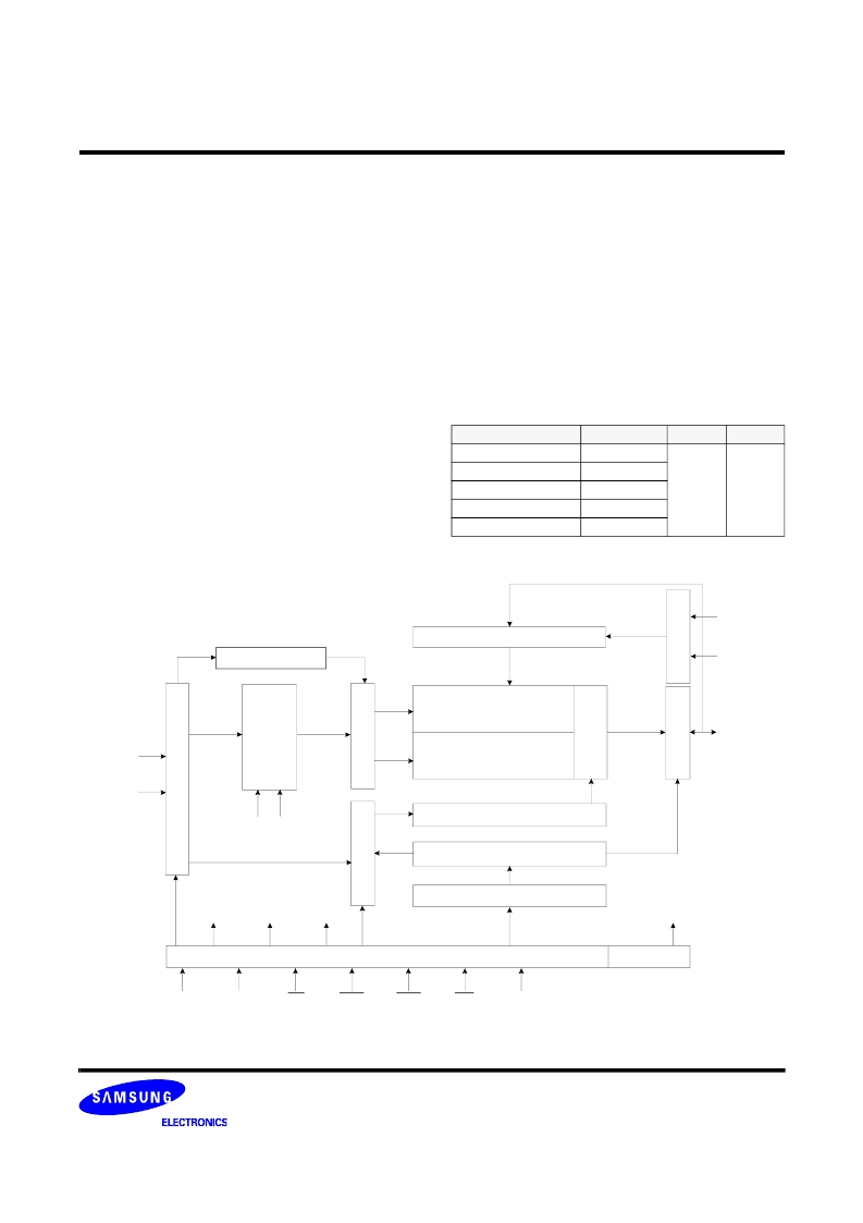
FUNCTIONAL BLOCK DIAGRAM
512K x 16Bit x 2 Banks Synchronous DRAM
ORDERING INFORMATION
Part NO.
MAX Freq.
183MHz
166MHz
143MHz
125MHz
100MHz
Interface Package
K4S161622E-TC55
K4S161622E-TC60
K4S161622E-TC70
K4S161622E-TC80
K4S161622E-TC10
LVTTL
50
TSOP(II)
* Samsung Electronics reserves the right to change products or specification without notice.
Bank Select
Data Input Register
512K x 16
512K x 16
S
O
I
Column Decoder
Latency & Burst Length
Programming Register
A
R
R
R
C
L
L
LCKE
LRAS
LCBR
LWE
LDQM
CLK
CKE
CS
RAS
CAS
WE
L(U)DQM
LWE
LDQM
DQi
CLK
ADD
LCAS
LWCBR
Timing Register
相關(guān)PDF資料 |
PDF描述 |
|---|---|
| K4S161622E-TC10 | 1M x 16 SDRAM |
| K4S161622E-TC55 | 1M x 16 SDRAM |
| K4S161622E-TC60 | 1M x 16 SDRAM |
| K4S161622E-TC70 | 1M x 16 SDRAM |
| K4S161622E-TC80 | 1M x 16 SDRAM |
相關(guān)代理商/技術(shù)參數(shù) |
參數(shù)描述 |
|---|---|
| K4S161622E-TC10 | 制造商:SAMSUNG 制造商全稱:Samsung semiconductor 功能描述:1M x 16 SDRAM |
| K4S161622E-TC55 | 制造商:SAMSUNG 制造商全稱:Samsung semiconductor 功能描述:1M x 16 SDRAM |
| K4S161622ETC60 | 制造商:SAMSUNG 功能描述:NEW |
| K4S161622E-TC60 | 制造商:SAMSUNG 制造商全稱:Samsung semiconductor 功能描述:1M x 16 SDRAM |
| K4S161622E-TC70 | 制造商:SAMSUNG 制造商全稱:Samsung semiconductor 功能描述:1M x 16 SDRAM |
發(fā)布緊急采購,3分鐘左右您將得到回復(fù)。