- 您現(xiàn)在的位置:買賣IC網(wǎng) > PDF目錄373086 > K8D6316UBM-YI08 (SAMSUNG SEMICONDUCTOR CO. LTD.) 64M Bit (8M x8/4M x16) Dual Bank NOR Flash Memory PDF資料下載
參數(shù)資料
| 型號: | K8D6316UBM-YI08 |
| 廠商: | SAMSUNG SEMICONDUCTOR CO. LTD. |
| 元件分類: | DRAM |
| 英文描述: | 64M Bit (8M x8/4M x16) Dual Bank NOR Flash Memory |
| 中文描述: | 6400位(800萬x8/4M x16)的雙銀行NOR閃存 |
| 文件頁數(shù): | 13/48頁 |
| 文件大小: | 767K |
| 代理商: | K8D6316UBM-YI08 |
第1頁第2頁第3頁第4頁第5頁第6頁第7頁第8頁第9頁第10頁第11頁第12頁當(dāng)前第13頁第14頁第15頁第16頁第17頁第18頁第19頁第20頁第21頁第22頁第23頁第24頁第25頁第26頁第27頁第28頁第29頁第30頁第31頁第32頁第33頁第34頁第35頁第36頁第37頁第38頁第39頁第40頁第41頁第42頁第43頁第44頁第45頁第46頁第47頁第48頁
NOR FLASH MEMORY
K8D6x16UTM / K8D6x16UBM
Revision 1.6
September, 2006
13
PRODUCT INTRODUCTION
The K8D6316U is an 64Mbit (67,108,864 bits) NOR-type Flash memory. The device features single voltage power supply operating
within the range of 2.7V to 3.6V. The device is programmed by using the Channel Hot Electron (CHE) injection mechanism which is
used to program EPROMs. The device is erased electrically by using Fowler-Nordheim tunneling mechanism. To provide highly flex-
ible erase and program capability, the device adapts a block memory architecture that divides its memory array into 135 blocks (64-
Kbyte x 127 , 8-Kbyte x 8). Programming is done in units of 8 bits (Byte) or 16 bits (Word). All bits of data in one or multiple blocks
can be erased simultaneously when the device executes the erase operation. To prevent the device from accidental erasing or over-
writing the programmed data, 135 memory blocks can be hardware protected by the block group. Byte/Word modes are available for
read operation. These modes can be selected via BYTE pin. The device provides read access times of 70ns, 80ns and 90ns support-
ing high speed microprocessors to operate without any wait states.
The command set of K8D6316U is fully compatible with standard Flash devices. The device is controlled by chip enable (CE), output
enable (OE) and write enable (WE). Device operations are executed by selective command codes. The command codes to be com-
bined with addresses and data are sequentially written to the command registers using microprocessor write timing.
The command
codes serve as inputs to an internal state machine which controls the program/erase circuitry. Register contents also internally latch
addresses and data necessary to execute the program and erase operations. The K8D6316U is implemented with Internal Program/
Erase Algorithms to execute the program/erase operations. The Internal Program/Erase Algorithms are invoked by program/erase
command sequences. The Internal Program Algorithm automatically programs and verifies data at specified addresses. The Internal
Erase Algorithm automatically pre-programs the memory cell which is not programmed and then executes the erase operation. The
K8D6316U has means to indicate the status of completion of program/erase operations. The status can be indicated via the RY/BY
pin, Data polling of DQ7, or the Toggle bit (DQ6). Once the operations have been completed, the device automatically resets itself to
the read mode. The device requires only 14 mA as active read current and 15 mA for program/erase operations.
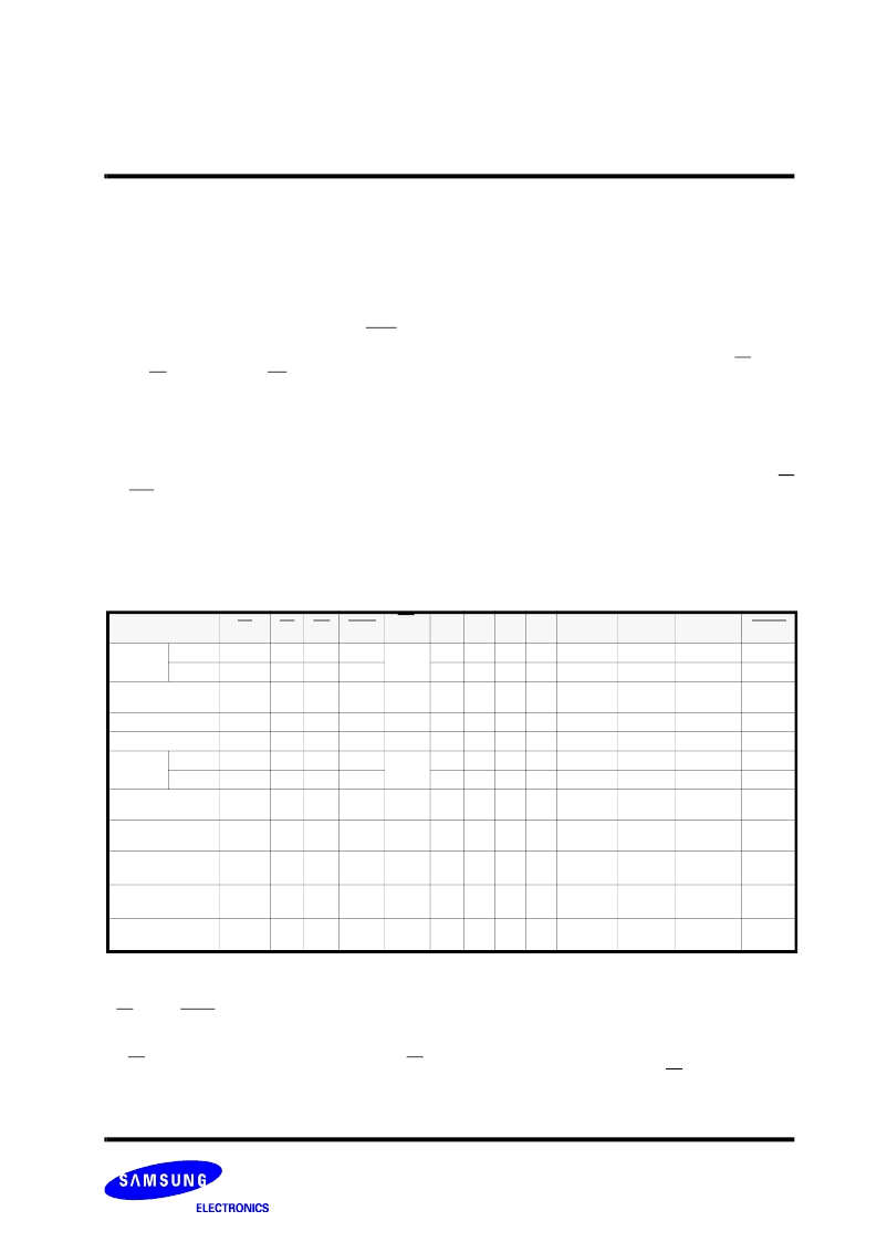
Table 7. Operations Table
Operation
CE
OE
WE
BYTE
WP/
ACC
A9
A6
A1
A0
DQ15/
A-1
DQ8/
DQ14
DQ0/
DQ7
RESET
Read
word
L
L
H
H
L/H
A9
A6
A1
A0
DQ15
D
OUT
D
OUT
H
byte
L
L
H
L
A9
A6
A1
A0
A-1
High-Z
D
OUT
H
Stand-by
Vcc
±
0.3V
X
X
X
(2)
X
X
X
X
High-Z
High-Z
High-Z
(2)
Output Disable
L
H
H
X
L/H
X
X
X
X
High-Z
High-Z
High-Z
H
Reset
X
X
X
X
L/H
X
X
X
X
High-Z
High-Z
High-Z
L
Write
word
L
H
L
H
(4)
A9
A6
A1
A0
D
IN
D
IN
D
IN
H
byte
L
H
L
L
A9
A6
A1
A0
A-1
High-Z
D
IN
H
Enable Block Group
Protect (3)
L
H
L
X
L/H
X
L
H
L
X
X
D
IN
V
ID
Enable Block Group
Unprotect (3)
L
H
L
X
(4)
X
H
H
L
X
X
D
IN
V
ID
Temporary Block
Group
X
X
X
X
(4)
X
X
X
X
X
X
X
V
ID
Auto Select
Manufacturer ID (5)
L
L
H
X
L/H
V
ID
L
L
L
X
X
Code
(See
Table 9)
H
Auto Select
Device Code (5)
L
L
H
X
L/H
V
ID
L
L
H
X
X
Code
(See
Table 9)
H
Notes :
1. L = V
IL
(Low), H = V
IH
(High), V
ID
= 8.5V~12.5V, D
IN
= Data in, D
OUT
= Data out, X = Don't care.
2. WP/ACC and RESET pin are asserted at Vcc
±
0.3 V or Vss
±
0.3 V in the Stand-by mode.
3. Addresses must be composed of the Block address (A12 - A21).
The Block Protect and Unprotect operations may be implemented via programming equipment too.
Refer to the "Block Group Protection and Unprotection".
4. If WP/ACC
=
V
IL,
the two outermost boot blocks is protected. If WP/ACC
=
V
IH,
the two outermost boot block protection depends on whether those
blocks were last protected or unprotected using the method described in "Block Group Protection and Unprotection". If WP/ACC
=
V
HH
, all blocks
will be temporarily unprotected.
5. Manufacturer and device codes may also be accessed via a command register write sequence. Refer to Table 9.
相關(guān)PDF資料 |
PDF描述 |
|---|---|
| K8D6316UBM-YI09 | 64M Bit (8M x8/4M x16) Dual Bank NOR Flash Memory |
| K8D6316UTM-FI09 | 64M Bit (8M x8/4M x16) Dual Bank NOR Flash Memory |
| K9E2G08U0M | 256M x 8 Bits NAND Flash Memory |
| K9E2G08U0M-V | 256M x 8 Bits NAND Flash Memory |
| K9E2G08U0M-Y | 256M x 8 Bits NAND Flash Memory |
相關(guān)代理商/技術(shù)參數(shù) |
參數(shù)描述 |
|---|---|
| K8D6316UBM-YI09 | 制造商:SAMSUNG 制造商全稱:Samsung semiconductor 功能描述:64M Bit (8M x8/4M x16) Dual Bank NOR Flash Memory |
| K8D6316UTM-DC07 | 制造商:SAMSUNG 制造商全稱:Samsung semiconductor 功能描述:64M Bit (8M x8/4M x16) Dual Bank NOR Flash Memory |
| K8D6316UTM-DC08 | 制造商:SAMSUNG 制造商全稱:Samsung semiconductor 功能描述:64M Bit (8M x8/4M x16) Dual Bank NOR Flash Memory |
| K8D6316UTM-DC09 | 制造商:SAMSUNG 制造商全稱:Samsung semiconductor 功能描述:64M Bit (8M x8/4M x16) Dual Bank NOR Flash Memory |
| K8D6316UTM-DI07 | 制造商:SAMSUNG 制造商全稱:Samsung semiconductor 功能描述:64M Bit (8M x8/4M x16) Dual Bank NOR Flash Memory |
發(fā)布緊急采購,3分鐘左右您將得到回復(fù)。