- 您現(xiàn)在的位置:買賣IC網(wǎng) > PDF目錄373087 > K9F2G08Q0M (SAMSUNG SEMICONDUCTOR CO. LTD.) FLASH MEMORY PDF資料下載
參數(shù)資料
| 型號: | K9F2G08Q0M |
| 廠商: | SAMSUNG SEMICONDUCTOR CO. LTD. |
| 英文描述: | FLASH MEMORY |
| 中文描述: | 閃存 |
| 文件頁數(shù): | 10/38頁 |
| 文件大?。?/td> | 601K |
| 代理商: | K9F2G08Q0M |
第1頁第2頁第3頁第4頁第5頁第6頁第7頁第8頁第9頁當(dāng)前第10頁第11頁第12頁第13頁第14頁第15頁第16頁第17頁第18頁第19頁第20頁第21頁第22頁第23頁第24頁第25頁第26頁第27頁第28頁第29頁第30頁第31頁第32頁第33頁第34頁第35頁第36頁第37頁第38頁
FLASH MEMORY
10
Preliminary
K9F2G08Q0M K9F2G16Q0M
K9F2G08U0M K9F2G16U0M
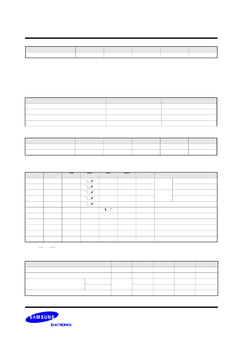
CAPACITANCE
(
T
A
=25
°
C, V
CC
=1.8V/3.3V, f=1.0MHz)
NOTE
: Capacitance is periodically sampled and not 100% tested.
Item
Symbol
Test Condition
Min
Max
Unit
Input/Output Capacitance
C
I/O
V
IL
=0V
-
10
pF
Input Capacitance
C
IN
V
IN
=0V
-
10
pF
VALID BLOCK
NOTE
:
1. The
device
may include invalid blocks when first shipped. Additional invalid blocks may develop while being used. The number of valid blocks is pre-
sented with both cases of invalid blocks considered. Invalid blocks are defined as blocks that contain one or more bad bits
. Do not erase or pro-
gram factory-marked bad blocks.
Refer to the attached technical notes for appropriate management of invalid blocks.
2. The 1st block, which is placed on 00h block address, is guaranteed to be a valid block, does not require Error Correction up to 1K program/erase
cycles.
Parameter
Symbol
Min
Typ.
Max
Unit
Valid Block Number
N
VB
2,008
-
2,048
Blocks
AC TEST CONDITION
(K9F2GXXX0M-XCB0 :TA=0 to 70
°
C, K9F2GXXX0M-XIB0:TA=-40 to 85
°
C
K9F2GXXQ0M : Vcc=1.70V~1.95V , K9F2GXXU0M : Vcc=2.7V~3.6V unless otherwise noted)
Parameter
K9F2GXXQ0M
K9F2GXXU0M
Input Pulse Levels
0V to Vcc
0V to Vcc
Input Rise and Fall Times
5ns
5ns
Input and Output Timing Levels
Vcc/2
Vcc/2
Output Load
1 TTL GATE and CL=30pF
1 TTL GATE and CL=50pF
Program / Erase Characteristics
NOTE
: 1. Max. time of
t
CBSY
depends on timing between internal program completion and data in
Parameter
Symbol
Min
Typ
Max
Unit
Program Time
t
PROG
-
300
700
μ
s
μ
s
Dummy Busy Time for Cache Program
t
CBSY
3
700
Number of Partial Program Cycles
in the Same Page
Main Array
Nop
-
-
4
cycles
Spare Array
-
-
4
cycles
Block Erase Time
t
BERS
-
2
3
ms
MODE SELECTION
NOTE
: 1. X can be V
IL
or V
IH.
2. WP and PRE should be biased to CMOS high or CMOS low for standby.
CLE
ALE
CE
WE
RE
WP
PRE
Mode
H
L
L
H
X
X
Read Mode Command Input
Address Input(5clock)
L
H
L
H
X
X
H
L
L
H
H
X
Write Mode Command Input
Address Input(5clock)
L
H
L
H
H
X
L
L
L
H
H
X
Data Input
L
L
L
H
X
X
Data Output
X
X
X
X
H
X
X
During Read(Busy)
X
X
X
X
X
H
X
During Program(Busy)
X
X
X
X
X
H
X
During Erase(Busy)
X
X
(1)
X
X
X
L
X
Write Protect
X
X
H
X
X
0V/V
CC
(2)
0V/V
CC
(2)
Stand-by
相關(guān)PDF資料 |
PDF描述 |
|---|---|
| K9F2G16Q0M | FLASH MEMORY |
| K9F5608D0C | TV 37C 37#16 PIN RECP |
| K9F5616D0C | 32M x 8 Bit , 16M x 16 Bit NAND Flash Memory |
| K9F5616D0C-D | 32M x 8 Bit , 16M x 16 Bit NAND Flash Memory |
| K9F5616D0C-H | 32M x 8 Bit , 16M x 16 Bit NAND Flash Memory |
相關(guān)代理商/技術(shù)參數(shù) |
參數(shù)描述 |
|---|---|
| K9F2G08R0A | 制造商:SAMSUNG 制造商全稱:Samsung semiconductor 功能描述:FLASH MEMORY |
| K9F2G08R0A-J | 制造商:SAMSUNG 制造商全稱:Samsung semiconductor 功能描述:FLASH MEMORY |
| K9F2G08U0A | 制造商:SAMSUNG 制造商全稱:Samsung semiconductor 功能描述:FLASH MEMORY |
| K9F2G08U0A-I | 制造商:SAMSUNG 制造商全稱:Samsung semiconductor 功能描述:FLASH MEMORY |
| K9F2G08U0A-IIB0T00 | 制造商:Samsung SDI 功能描述: |
發(fā)布緊急采購,3分鐘左右您將得到回復(fù)。