- 您現(xiàn)在的位置:買賣IC網(wǎng) > PDF目錄373087 > K9F2G08Q0M (SAMSUNG SEMICONDUCTOR CO. LTD.) FLASH MEMORY PDF資料下載
參數(shù)資料
| 型號: | K9F2G08Q0M |
| 廠商: | SAMSUNG SEMICONDUCTOR CO. LTD. |
| 英文描述: | FLASH MEMORY |
| 中文描述: | 閃存 |
| 文件頁數(shù): | 32/38頁 |
| 文件大?。?/td> | 601K |
| 代理商: | K9F2G08Q0M |
第1頁第2頁第3頁第4頁第5頁第6頁第7頁第8頁第9頁第10頁第11頁第12頁第13頁第14頁第15頁第16頁第17頁第18頁第19頁第20頁第21頁第22頁第23頁第24頁第25頁第26頁第27頁第28頁第29頁第30頁第31頁當前第32頁第33頁第34頁第35頁第36頁第37頁第38頁
FLASH MEMORY
32
Preliminary
K9F2G08Q0M K9F2G16Q0M
K9F2G08U0M K9F2G16U0M
Cache Program
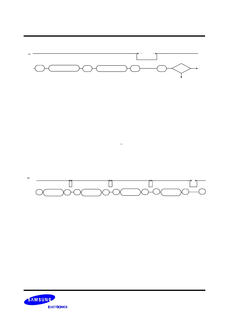
Cache Program is an extension of Page Program, which is executed with 2112byte(X8 device) or 1056word(X16 device) data regis-
ters, and is available only within a block. Since the device has 1 page of cache memory, serial data input may be executed while data
stored in data register are programmed into memory cell.
Figure 9. Random Data Input In a Page
80h
R/B
Address & Data Input
I/O
0
Pass
10h
70h
Fail
t
PROG
85h
Address & Data Input
After writing the first set of data up to 2112byte(X8 device) or 1056word(X16 device) into the selected cache registers, Cache Pro-
gram command (15h) instead of actual Page Program (10h) is inputted to make cache registers free and to start internal program
operation. To transfer data from cache registers to data registers, the device remains in Busy state for a short period of time(tCBSY)
and has its cache registers ready for the next data-input while the internal programming gets started with the data loaded into data
registers. Read Status command (70h) may be issued to find out when cache registers become ready by polling the Cache-Busy sta-
tus bit(I/O 6). Pass/fail status of only the previouse page is available upon the return to Ready state. When the next set of data is
inputted with the Cache Program command, tCBSY is affected by the progress of pending internal programming. The programming of
the cache registers is initiated only when the pending program cycle is finished and the data registers are available for the transfer of
data from cache registers. The status bit(I/O5) for internal Ready/Busy may be polled to identify the completion of internal program-
ming. If the system monitors the progress of programming only with R/B, the last page of the target programming sequence must be
progammed with actual Page Program command (10h).
Figure 10. Cache Program
(available only within a block)
t
CBSY
80h
R/B
80h
Address &
Data Input
15h
80h
Address &
Data Input
15h
80h
Address &
Data Input
10h
t
CBSY
t
CBSY
t
PROG
70h
Address &
Data Input*
15h
I/Ox
Col Add1,2 & Row Add1,2,3
Data
Col Add1,2
Data
Col Add1,2 & Row Add1,2,3
Data
Col Add1,2 & Row Add1,2,3
Data
Col Add1,2 & Row Add1,2,3
Data
Col Add1,2 & Row Add1,2,3
Data
"0"
"1"
相關(guān)PDF資料 |
PDF描述 |
|---|---|
| K9F2G16Q0M | FLASH MEMORY |
| K9F5608D0C | TV 37C 37#16 PIN RECP |
| K9F5616D0C | 32M x 8 Bit , 16M x 16 Bit NAND Flash Memory |
| K9F5616D0C-D | 32M x 8 Bit , 16M x 16 Bit NAND Flash Memory |
| K9F5616D0C-H | 32M x 8 Bit , 16M x 16 Bit NAND Flash Memory |
相關(guān)代理商/技術(shù)參數(shù) |
參數(shù)描述 |
|---|---|
| K9F2G08R0A | 制造商:SAMSUNG 制造商全稱:Samsung semiconductor 功能描述:FLASH MEMORY |
| K9F2G08R0A-J | 制造商:SAMSUNG 制造商全稱:Samsung semiconductor 功能描述:FLASH MEMORY |
| K9F2G08U0A | 制造商:SAMSUNG 制造商全稱:Samsung semiconductor 功能描述:FLASH MEMORY |
| K9F2G08U0A-I | 制造商:SAMSUNG 制造商全稱:Samsung semiconductor 功能描述:FLASH MEMORY |
| K9F2G08U0A-IIB0T00 | 制造商:Samsung SDI 功能描述: |
發(fā)布緊急采購,3分鐘左右您將得到回復(fù)。