- 您現(xiàn)在的位置:買賣IC網(wǎng) > PDF目錄373087 > K9F5608U0 (SAMSUNG SEMICONDUCTOR CO. LTD.) TV 6C 6#12 PIN WALL RECP PDF資料下載
參數(shù)資料
| 型號: | K9F5608U0 |
| 廠商: | SAMSUNG SEMICONDUCTOR CO. LTD. |
| 英文描述: | TV 6C 6#12 PIN WALL RECP |
| 中文描述: | 32M的× 8位NAND閃存 |
| 文件頁數(shù): | 2/29頁 |
| 文件大小: | 610K |
| 代理商: | K9F5608U0 |
第1頁當(dāng)前第2頁第3頁第4頁第5頁第6頁第7頁第8頁第9頁第10頁第11頁第12頁第13頁第14頁第15頁第16頁第17頁第18頁第19頁第20頁第21頁第22頁第23頁第24頁第25頁第26頁第27頁第28頁第29頁
K9F5608U0A-YCB0,K9F5608U0A-YIB0
FLASH MEMORY
2
32M x 8 Bit NAND Flash Memory
The K9F5608U0A are a 32M(33,554,432)x8bit NAND Flash
Memory with a spare 1,024K(1,048,576)x8bit. Its NAND cell
provides the most cost-effective solution for the solid state
mass storage market. A program operation programs the 528-
byte page in typical 200
μ
s and an erase operation can be per-
formed in typical 2ms on a 16K-byte block. Data in the page
can be read out at 50ns cycle time per byte. The I/O pins serve
as the ports for address and data input/output as well as com-
mand inputs. The on-chip write controller automates all pro-
gram and erase functions including pulse repetition, where
required, and internal verification and margining of data. Even
the write-intensive systems can take advantage of the
K9F5608U0A
′
s extended reliability of 100K program/erase
cycles by providing ECC(Error Correcting Code) with real time
mapping-out algorithm.
The K9F5608U0A-YCB0/YIB0 is an optimum solution for large
nonvolatile storage applications such as solid state file storage
and other portable applications requiring non-volatility.
GENERAL DESCRIPTION
FEATURES
Voltage Supply : 2.7V~3.6V
Organization
- Memory Cell Array : (32M + 1024K)bit x 8bit
- Data Register : (512 + 16)bit x8bit
Automatic Program and Erase
- Page Program : (512 + 16)Byte
- Block Erase : (16K + 512)Byte
528-Byte Page Read Operation
- Random Access : 10
μ
s(Max.)
- Serial Page Access : 50ns(Min.)
Fast Write Cycle Time
- Program time : 200
μ
s(Typ.)
- Block Erase Time : 2ms(Typ.)
Command/Address/Data Multiplexed I/O Port
Hardware Data Protection
- Program/Erase Lockout During Power Transitions
Reliable CMOS Floating-Gate Technology
- Endurance : 100K Program/Erase Cycles
- Data Retention : 10 Years
Command Register Operation
Intelligent Copy-Back
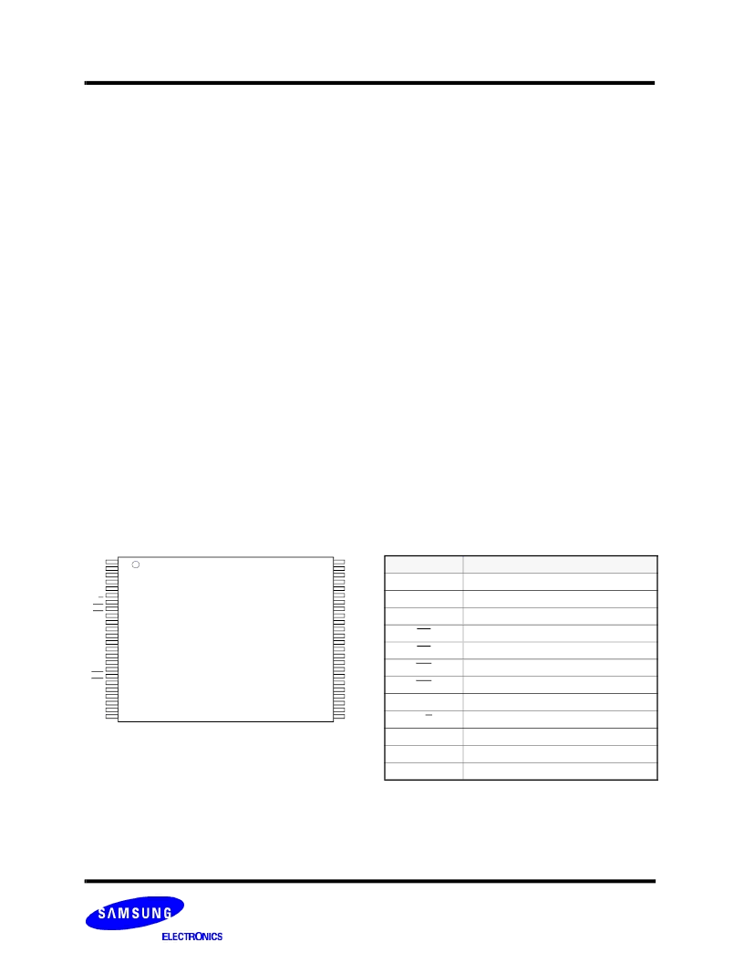
Package :
- K9F5608U0A-YCB0/YIB0 :
48 - Pin TSOP I (12 x 20 / 0.5 mm pitch)
PIN CONFIGURATION
NOTE
: Connect all V
CC
and V
SS
pins of each device to common power supply outputs.
Do not leave V
CC
or V
SS
disconnected.
K9F5608U0A-YCB0/YIB0
1
2
3
4
5
6
7
8
9
10
11
12
13
14
15
16
17
18
19
20
21
22
23
24
48
47
46
45
44
43
42
41
40
39
38
37
36
35
34
33
32
31
30
29
28
27
26
25
R/B
CE
Vcc
Vss
WE
WP
N.C
N.C
Pin Name
Pin Function
I/O
0
~ I/O
7
Data Input/Outputs
CLE
Command Latch Enable
ALE
Address Latch Enable
CE
Chip Enable
RE
Read Enable
WE
Write Enable
WP
Write Protect
GND
GND input for enabling spare area
R/B
Ready/Busy output
V
CC
Power
V
SS
Ground
N.C
No Connection
PIN DESCRIPTION
相關(guān)PDF資料 |
PDF描述 |
|---|---|
| K9F5608U0A | TV 6C 6#12 PIN RECP |
| K9F5608U0A-YCB0 | TV 16C 16#16 PIN RECP |
| K9F5608U0A-YIB0 | TV 79C 79#22D PIN RECP |
| K9F6408U0C-T | 8M x 8 Bit NAND Flash Memory |
| K9F6408U0C-V | 8M x 8 Bit NAND Flash Memory |
相關(guān)代理商/技術(shù)參數(shù) |
參數(shù)描述 |
|---|---|
| K9F5608U0A | 制造商:SAMSUNG 制造商全稱:Samsung semiconductor 功能描述:32M x 8 Bit NAND Flash Memory |
| K9F5608U0A-YCB0 | 制造商:SAMSUNG 制造商全稱:Samsung semiconductor 功能描述:32M x 8 Bit NAND Flash Memory |
| K9F5608U0A-YIB0 | 制造商:SAMSUNG 制造商全稱:Samsung semiconductor 功能描述:32M x 8 Bit NAND Flash Memory |
| K9F5608U0B | 制造商:SAMSUNG 制造商全稱:Samsung semiconductor 功能描述:32M x 8 Bit , 16M x 16 Bit NAND Flash Memory |
| K9F5608U0B-DCB0 | 制造商:SAMSUNG 制造商全稱:Samsung semiconductor 功能描述:32M x 8 Bit , 16M x 16 Bit NAND Flash Memory |
發(fā)布緊急采購,3分鐘左右您將得到回復(fù)。