- 您現(xiàn)在的位置:買賣IC網(wǎng) > PDF目錄373088 > K9K2G08Q0M (SAMSUNG SEMICONDUCTOR CO. LTD.) ER 19C 19#12 SKT PLUG PDF資料下載
參數(shù)資料
| 型號: | K9K2G08Q0M |
| 廠商: | SAMSUNG SEMICONDUCTOR CO. LTD. |
| 英文描述: | ER 19C 19#12 SKT PLUG |
| 中文描述: | 256M × 8位/ 128M的× 16位NAND閃存 |
| 文件頁數(shù): | 8/40頁 |
| 文件大?。?/td> | 641K |
| 代理商: | K9K2G08Q0M |
第1頁第2頁第3頁第4頁第5頁第6頁第7頁當(dāng)前第8頁第9頁第10頁第11頁第12頁第13頁第14頁第15頁第16頁第17頁第18頁第19頁第20頁第21頁第22頁第23頁第24頁第25頁第26頁第27頁第28頁第29頁第30頁第31頁第32頁第33頁第34頁第35頁第36頁第37頁第38頁第39頁第40頁
FLASH MEMORY
8
K9W4G08U1M
K9K2G08U0M
K9W4G16U1M
K9K2G16Q0M
K9K2G16U0M
K9K2G08Q0M
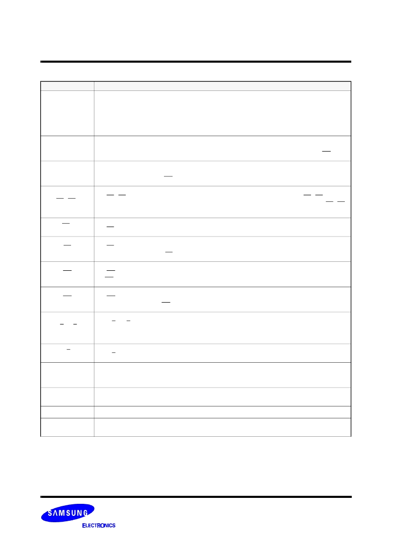
PIN DESCRIPTION
NOTE
: Connect all V
CC
and V
SS
pins of each device to common power supply outputs.
Do not leave V
CC
or V
SS
disconnected.
Pin Name
Pin Function
I/O
0
~ I/O
7
(K9K2G08X0M)
I/O
0
~ I/O
15
(K9K2G16X0M)
DATA INPUTS/OUTPUTS
The I/O pins are used to input command, address and data, and to output data during read operations. The I/
O pins float to high-z when the chip is deselected or when the outputs are disabled.
I/O8 ~ I/O15 are used only in X16 organization device. Since command input and address input are x8 oper-
ation, I/O8 ~ I/O15 are not used to input command & address. I/O8 ~ I/O15 are used only for data input and
output.
CLE
COMMAND LATCH ENABLE
The CLE input controls the activating path for commands sent to the command register. When active high,
commands are latched into the command register through the I/O ports on the rising edge of the WE signal.
ALE
ADDRESS LATCH ENABLE
The ALE input controls the activating path for address to the internal address registers. Addresses are
latched on the rising edge of WE with ALE high.
CE / CE1
CHIP ENABLE
The CE / CE1 input is the device selection control. When the device is in the Busy state, CE / CE1 high is
ignored, and the device does not return to standby mode in program or erase opertion. Regarding CE / CE1
control during read operation, refer to ’Page read’ section of Device operation .
CE2
CHIP ENABLE
The CE2 input enables the second K9K2GXXU0M
RE
READ ENABLE
The RE input is the serial data-out control, and when active drives the data onto the I/O bus. Data is valid
tREA after the falling edge of RE which also increments the internal column address counter by one.
WE
WRITE ENABLE
The WE input controls writes to the I/O port. Commands, address and data are latched on the rising edge of
the WE pulse.
WP
WRITE PROTECT
The WP pin provides inadvertent write/erase protection during power transitions. The internal high voltage
generator is reset when the WP pin is active low.
R/B / R/B1
READY/BUSY OUTPUT
The R/B / R/B1 output indicates the status of the device operation. When low, it indicates that a program,
erase or random read operation is in process and returns to high state upon completion. It is an open drain
output and does not float to high-z condition when the chip is deselected or when outputs are disabled.
R/B2
READY/BUSY OUTPUT
The R/B2 output indicates the status of the second K9K2GXXU0M
PRE
POWER-ON READ ENABLE
The PRE controls auto read operation executed during power-on. The power-on auto-read is enabled when
PRE pin is tied to Vcc.
Vcc
POWER
V
CC
is the power supply for device.
Vss
GROUND
N.C
NO CONNECTION
Lead is not internally connected.
相關(guān)PDF資料 |
PDF描述 |
|---|---|
| K9K2G16Q0M | 256M x 8 Bit / 128M x 16 Bit NAND Flash Memory |
| K9K4G08U1M | 256M x 8 Bit / 128M x 16 Bit / 512M x 8 Bit NAND Flash Memory |
| K9S1208V0M-SSB0 | 64M x 8 Bit SmartMedia Card |
| K9S1208V0 | 64MB & 128MB SmartMediaTM Card |
| K9D1G08V0M | 64MB & 128MB SmartMediaTM Card |
相關(guān)代理商/技術(shù)參數(shù) |
參數(shù)描述 |
|---|---|
| K9K2G08Q0M-P | 制造商:SAMSUNG 制造商全稱:Samsung semiconductor 功能描述:256M x 8 Bit / 128M x 16 Bit NAND Flash Memory |
| K9K2G08Q0M-PCB0 | 制造商:SAMSUNG 制造商全稱:Samsung semiconductor 功能描述:256M x 8 Bit / 128M x 16 Bit NAND Flash Memory |
| K9K2G08Q0M-PIB0 | 制造商:SAMSUNG 制造商全稱:Samsung semiconductor 功能描述:256M x 8 Bit / 128M x 16 Bit NAND Flash Memory |
| K9K2G08Q0M-Y | 制造商:SAMSUNG 制造商全稱:Samsung semiconductor 功能描述:256M x 8 Bit / 128M x 16 Bit NAND Flash Memory |
| K9K2G08Q0M-YCB0 | 制造商:SAMSUNG 制造商全稱:Samsung semiconductor 功能描述:256M x 8 Bit / 128M x 16 Bit NAND Flash Memory |
發(fā)布緊急采購,3分鐘左右您將得到回復(fù)。