- 您現(xiàn)在的位置:買賣IC網(wǎng) > PDF目錄373088 > K9K2G08U0M-FIB0 (SAMSUNG SEMICONDUCTOR CO. LTD.) 256M x 8 Bit / 128M x 16 Bit NAND Flash Memory PDF資料下載
參數(shù)資料
| 型號(hào): | K9K2G08U0M-FIB0 |
| 廠商: | SAMSUNG SEMICONDUCTOR CO. LTD. |
| 英文描述: | 256M x 8 Bit / 128M x 16 Bit NAND Flash Memory |
| 中文描述: | 256M × 8位/ 128M的× 16位NAND閃存 |
| 文件頁數(shù): | 31/38頁 |
| 文件大?。?/td> | 734K |
| 代理商: | K9K2G08U0M-FIB0 |
第1頁第2頁第3頁第4頁第5頁第6頁第7頁第8頁第9頁第10頁第11頁第12頁第13頁第14頁第15頁第16頁第17頁第18頁第19頁第20頁第21頁第22頁第23頁第24頁第25頁第26頁第27頁第28頁第29頁第30頁當(dāng)前第31頁第32頁第33頁第34頁第35頁第36頁第37頁第38頁
FLASH MEMORY
31
K9K2G08Q0M-YCB0,YIB0,PCB0,PIB0
K9K2G08U0M-YCB0,YIB0,PCB0,PIB0
K9K2G16Q0M-YCB0,YIB0,PCB0,PIB0
K9K2G16U0M-YCB0,YIB0,PCB0,PIB0
K9K2G08U0M-VCB0,VIB0,FCB0,FIB0
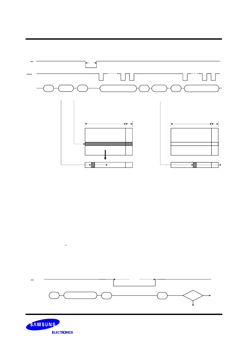
Figure 7. Random Data Output In a Page
Address
5Cycles
00h
Data Output
R/B
RE
t
R
30h
Address
2Cycles
05h
E0h
Data Output
Data Field
Spare Field
Data Field
Spare Field
PAGE PROGRAM
The device is programmed basically on a page basis, but it does allow multiple partial page programing of a word or consecutive
bytes up to 2112(X8 device) or words up to 1056(X16 device), in a single page program cycle. The number of consecutive partial
page programming operation within the same page without an intervening erase operation must not exceed 4 times for main array(X8
device:1time/512byte, X16 device:1time/256word) and 4 times for spare array(X8 device:1time/16byte, X16 device:1time/8word). The
addressing should be done in sequential order in a block. A page program cycle consists of a serial data loading period in which up to
2112bytes(X8 device) or 1056words(X16 device) of data may be loaded into the data register, followed by a non-volatile programming
period where the loaded data is programmed into the appropriate cell.
The serial data loading period begins by inputting the Serial Data Input command(80h), followed by the five cycle address inputs and
then serial data loading. The words other than those to be programmed do not need to be loaded. The device supports random data
input in a page. The column address for the next data, which will be entered, may be changed to the address which follows random
data input command(85h). Random data input may be operated multiple times regardless of how many times it is done in a page.
The Page Program confirm command(10h) initiates the programming process. Writing 10h alone without previously entering the serial
data will not initiate the programming process. The internal write state controller automatically executes the algorithms and timings
necessary for program and verify, thereby freeing the system controller for other tasks. Once the program process starts, the Read
Status Register command may be entered to read the status register. The system controller can detect the completion of a program
cycle by monitoring the R/B output, or the Status bit(I/O 6) of the Status Register. Only the Read Status command and Reset com-
mand are valid while programming is in progress. When the Page Program is complete, the Write Status Bit(I/O 0) may be
checked(Figure 8). The internal write verify detects only errors for "1"s that are not successfully programmed to "0"s. The command
register remains in Read Status command mode until another valid command is written to the command register.
Figure 8. Program & Read Status Operation
80h
R/B
Address & Data Input
I/O
0
Pass
Data
10h
70h
Fail
t
PROG
I/Ox
I/Ox
Col Add1,2 & Row Add1,2,3
"0"
"1"
Col Add1,2 & Row Add1,2,3
相關(guān)PDF資料 |
PDF描述 |
|---|---|
| K9K2G08U0M-PCB0 | 256M x 8 Bit / 128M x 16 Bit NAND Flash Memory |
| K9K2G08U0M-PIB0 | 256M x 8 Bit / 128M x 16 Bit NAND Flash Memory |
| K9K2G08U0M-VCB0 | 256M x 8 Bit / 128M x 16 Bit NAND Flash Memory |
| K9K2G08U0M-VIB0 | 256M x 8 Bit / 128M x 16 Bit NAND Flash Memory |
| K9K2G08U0M-YIB0 | 256M x 8 Bit / 128M x 16 Bit NAND Flash Memory |
相關(guān)代理商/技術(shù)參數(shù) |
參數(shù)描述 |
|---|---|
| K9K2G08U0M-PCB0 | 制造商:SAMSUNG 制造商全稱:Samsung semiconductor 功能描述:256M x 8 Bit / 128M x 16 Bit NAND Flash Memory |
| K9K2G08U0M-PCB000 | 制造商:Samsung Semiconductor 功能描述: |
| K9K2G08U0M-PIB0 | 制造商:SAMSUNG 制造商全稱:Samsung semiconductor 功能描述:256M x 8 Bit / 128M x 16 Bit NAND Flash Memory |
| K9K2G08U0M-V | 制造商:SAMSUNG 制造商全稱:Samsung semiconductor 功能描述:256M x 8 Bit / 128M x 16 Bit NAND Flash Memory |
| K9K2G08U0M-VCB0 | 制造商:SAMSUNG 制造商全稱:Samsung semiconductor 功能描述:256M x 8 Bit / 128M x 16 Bit NAND Flash Memory |
發(fā)布緊急采購,3分鐘左右您將得到回復(fù)。