- 您現(xiàn)在的位置:買賣IC網 > PDF目錄367494 > L9216A CAP CER 270PF 3.15KVDC R3 RAD PDF資料下載
參數資料
| 型號: | L9216A |
| 英文描述: | CAP CER 270PF 3.15KVDC R3 RAD |
| 中文描述: | 短環(huán)振鈴用戶接口與地面開始 |
| 文件頁數: | 37/48頁 |
| 文件大小: | 1062K |
| 代理商: | L9216A |
第1頁第2頁第3頁第4頁第5頁第6頁第7頁第8頁第9頁第10頁第11頁第12頁第13頁第14頁第15頁第16頁第17頁第18頁第19頁第20頁第21頁第22頁第23頁第24頁第25頁第26頁第27頁第28頁第29頁第30頁第31頁第32頁第33頁第34頁第35頁第36頁當前第37頁第38頁第39頁第40頁第41頁第42頁第43頁第44頁第45頁第46頁第47頁第48頁

Preliminary Data Sheet
September 2001
Short-Loop Ringing SLIC with Ground Start
L9216A/G
Agere Systems Inc.
37
ac Applications
(continued)
Design Examples
(continued)
First-Generation Codec ac Interface Network—
Complex Termination
The reference circuit in Figure 26 shows the complete
SLIC schematic for interface to the Agere T7504 first-
generation codec for the German complex termination
impedance. For this example, the ac interface was
designed for a 220
+ (820
|| 115 nF) complex
termination and hybrid balance with transmit gain and
receive gain set to 0 dBm. For illustration purposes,
1 Vrms PPM injection was assumed in this example.
This implies the overhead voltage is increased to
7.24 V and no meter pulse rejection is required. Also,
this example illustrates the device using fixed overhead
and current limit.
Complex Termination Impedance Design Example
The gain shaping necessary for a complex termination
impedance may be done by shaping across the AX
amplifier at nodes ITR and VTX.
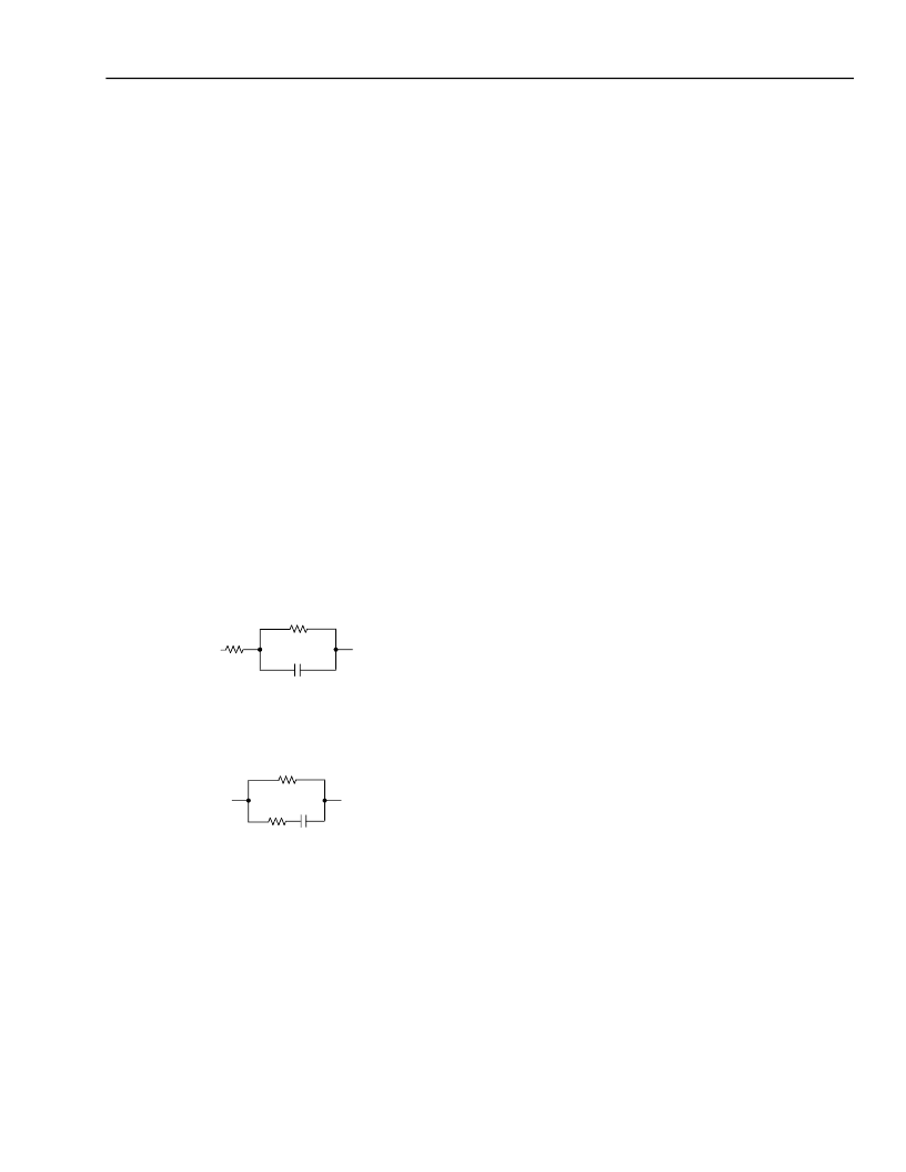
Complex termination is specified in the form:
5-6396(F)
To work with this application, convert termination to the
form:
5-6398(F)
where:
R
1
′ = R
1
+ R
2
1
R
2
R
2
′ =
(R
1
+ R
2
)
C′ =
C
ac Interface Using First-Generation Codec
R
GX
/R
TGS
/C
GS
(Z
TG
): these components give gain shap-
ing to get good gain flatness. These components are a
scaled version of the specified complex termination
impedance.
Note for pure (600
) resistive terminations, compo-
nents R
TGS
and C
GS
are not used. Resistor R
GX
is used
and is still 4750
.
R
X
/R
T6
: with other components set, the transmit gain
(for complex and resistive terminations) R
X
and R
T6
are
varied to give specified transmit gain.
R
T3
/R
RCV
/R
GP
: for both complex and resistive termina-
tions, the ratio of these resistors sets the receive gain.
For resistive terminations, the ratio of these resistors
sets the return loss characteristic. For complex termi-
nations, the ratio of these resistors sets the low-fre-
quency return loss characteristic.
C
N
/R
N1
/R
N2
: for complex terminations, these compo-
nents provide high-frequency compensation to the
return loss characteristic.
For resistive terminations, these components are not
used and RCVN is connected to ground via a resistor.
R
HB
: sets hybrid balance for all terminations.
Set Z
TG
—Gain Shaping:
Z
TG
= R
GX
|| R
TGS
+ C
GS
which is a scaled version of
Z
T/R
(the specified termination resistance) in the
R
1
′ || R
2
′ + C′ form.
R
GX
must be 4750
to set SLIC transconductance to
300 V/A.
R
GX
= 4750
At dc, C
GS
and C′ are open.
R
GX
= M x R
1
′
where M is the scale factor.
R
1
′
M =
It can be shown:
R
TGS
= M x R
2
′
and
C
TGS
=
R
2
C
R
1
R
1
′
C′
R
2
′
-------
+
R
1
R
2
---------------------
2
--------------
′
M
------
相關PDF資料 |
PDF描述 |
|---|---|
| L9217A | CAP CER 2700PF 3.15KVDC R3 RAD |
| L9218A | CAP CER 330PF 3.15KVDC R3 RAD |
| L9219A | CAP CER 390PF 3.15KVDC R3 RAD |
| L9310 | Line Interface and Line Access Circuit Full-Feature SLIC,Ringing Relay,and Test Access Device |
| L9311 | Line Interface and Line Access Circuit Full-Feature SLIC with High Longitudinal Balance, Ringing Relay,and GR-909 Test Access |
相關代理商/技術參數 |
參數描述 |
|---|---|
| L9217A | 制造商:AGERE 制造商全稱:AGERE 功能描述:Low-Cost Line Interface with Reverse Battery and PPM |
| L9218A | 制造商:AGERE 制造商全稱:AGERE 功能描述:Low-Cost Line Interface |
| L9219A | 制造商:AGERE 制造商全稱:AGERE 功能描述:Low-Cost Line Interface with Reverse Battery and Dual Current Limit |
| L9222 | 功能描述:功率驅動器IC Quad Inv Tran Switch RoHS:否 制造商:Micrel 產品:MOSFET Gate Drivers 類型:Low Cost High or Low Side MOSFET Driver 上升時間: 下降時間: 電源電壓-最大:30 V 電源電壓-最小:2.75 V 電源電流: 最大功率耗散: 最大工作溫度:+ 85 C 安裝風格:SMD/SMT 封裝 / 箱體:SOIC-8 封裝:Tube |
| L9222_04 | 制造商:STMICROELECTRONICS 制造商全稱:STMicroelectronics 功能描述:QUAD INVERTING TRANSISTOR SWITCH |
發(fā)布緊急采購,3分鐘左右您將得到回復。