- 您現(xiàn)在的位置:買賣IC網(wǎng) > PDF目錄358741 > LAN83C180 (STANDARD MICROSYSTEMS CORP) 10/100 FAST ETHERNET PHY TRANSCEIVER PDF資料下載
參數(shù)資料
| 型號: | LAN83C180 |
| 廠商: | STANDARD MICROSYSTEMS CORP |
| 元件分類: | 網(wǎng)絡(luò)接口 |
| 英文描述: | 10/100 FAST ETHERNET PHY TRANSCEIVER |
| 中文描述: | DATACOM, ETHERNET TRANSCEIVER, PQFP64 |
| 封裝: | 10 X 10 MM, 1 MM HEIGHT, PLASTIC, TQFP-64 |
| 文件頁數(shù): | 18/22頁 |
| 文件大小: | 166K |
| 代理商: | LAN83C180 |

SMSC DS – LAN83C180
Page 18
Rev. 08/24/2001
OPERATING CONDITIONS
MAXIMUM GUARANTEED RATINGS*
Operating Temperature Range .................................................................................................................0
o
C to +70
o
C
Storage Temperature Range ...............................................................................................................-40
o
C to +125
o
C
Lead Temperature Range (soldering, 10 seconds) .......................................................................................... +TBD
o
C
Positive Voltage on any pin, with respect to Ground .....................................................................................V
DD
+ 0.5V
Negative Voltage on any pin, with respect to Ground ............................................................................................-0.5V
Maximum V
DD
........................................................................................................................................................+7.0V
*Stresses above those listed above could cause permanent damage to the device. This is a stress rating only and
functional operation of the device at any other condition above those indicated in the operation sections of this
specification is not implied.
Note: When powering this device from laboratory or system power supplies, it is important that the Absolute
Maximum Ratings not be exceeded or device failure can result. Some power supplies exhibit voltage spikes on their
outputs when the AC power is switched on or off. In addition, voltage transients on the AC power line may appear
on the DC output. If this possibility exists, it is suggested that a clamp circuit be used.
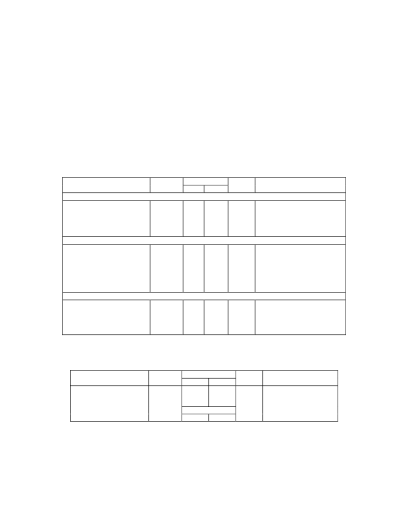
DC ELECTRICAL CHARACTERISTICS
(T
A
= 0
o
C - 70
o
C, V
DD
= +5.0V ±5%)
VALUE
MIN
CHARACTERISTIC
SYMBOL
DC PARAMETERS – INPUT
V
IH
V
IL
I
IH
I
IL
-
-
DC PARAMETERS - OUTPUT - 6MA BUFFERS
V
OH
V
OL
I
OH
I
OL
-
-
-
-
DC PARAMETERS – SUPPLY CURRENT
MAX
UNITS
CONDITIONS
High Level Input Voltage
High Level Input Voltage
High Level Input Current
High Level Input Current
Pin Capacitance To Ground
2
V
SS
-
V
0.8
1
-1
8
V
V
μA
μA
pF
No pull-up
including package
High Level Output Voltage
High Level Output Voltage
High Level Output Current
High Level Output Current
Rise Time
Fall Time
Pin Capacitance To Ground
4
V
SS
-
V
DD
0.4
-6
6
4
4
8
V
V
mA
mA
nS
nS
pF
0.4V to 2.4V into 20pF load
0.4V to 2.4V into 20pF load
10 Base-T Idle
10 Base-T Active
100 Base TX Mode
Auto Negotiation
Low Power
90
180
120
90
35
mA
mA
mA
mA
mA
Measured at 5V, room
temperature. These figures
include the current flowing in
the Transmit load resistors.
DIFFERENTIAL OUTPUT
Recommended operating conditions apply except where stated.
VALUE
MIN
2
-50
-
Typical = Vdd/2
-
CHARACTERISTIC
High level
Zero level
Low level
Current at
Slew rate
SYMBOL
MAX
-
50
-2
UNITS
V
mV
V
μA
V/ns
CONDITIONS
0.5
相關(guān)PDF資料 |
PDF描述 |
|---|---|
| LAN83C185 | HIGH PERFORMANCE SINGLE CHIP LOW POWER 10/100 ETHERNET PHYSICAL LAYER TRANSCEIVER |
| LAN83C183-JD | FAST ETHERNET PHYSICAL LAYER DEVICE |
| LAN83C180TQFP | 10/100 FAST ETHERNET PHY TRANSCEIVER |
| LAN83C183 | FAST ETHERNET PHYSICAL LAYER DEVICE |
| LAN83C185-JD | HIGH PERFORMANCE SINGLE CHIP LOW POWER 10/100 ETHERNET PHYSICAL LAYER TRANSCEIVER |
相關(guān)代理商/技術(shù)參數(shù) |
參數(shù)描述 |
|---|---|
| LAN83C180_01 | 制造商:SMSC 制造商全稱:SMSC 功能描述:10/100 Fast Ethernet PHY Transceiver |
| LAN83C180TQFP | 制造商:SMSC 制造商全稱:SMSC 功能描述:10/100 Fast Ethernet PHY Transceiver |
| LAN83C183 | 制造商:SMSC 制造商全稱:SMSC 功能描述:FAST ETHERNET PHYSICAL LAYER DEVICE |
| LAN83C183-JD | 制造商:SMSC 制造商全稱:SMSC 功能描述:FAST ETHERNET PHYSICAL LAYER DEVICE |
| LAN83C185 | 制造商:SMSC 制造商全稱:SMSC 功能描述:High Performance Single Chip Low Power 10/100 Ethernet Physical Layer Transceiver |
發(fā)布緊急采購,3分鐘左右您將得到回復(fù)。