- 您現(xiàn)在的位置:買賣IC網(wǎng) > PDF目錄377611 > LC5256MC-4F256C (LATTICE SEMICONDUCTOR CORP) 3.3V, 2.5V and 1.8V In-System Programmable eXpanded Programmable Logic Device XPLD⑩ Family PDF資料下載
參數(shù)資料
| 型號(hào): | LC5256MC-4F256C |
| 廠商: | LATTICE SEMICONDUCTOR CORP |
| 元件分類: | PLD |
| 英文描述: | 3.3V, 2.5V and 1.8V In-System Programmable eXpanded Programmable Logic Device XPLD⑩ Family |
| 中文描述: | EE PLD, 4.8 ns, PBGA256 |
| 封裝: | FPBGA-256 |
| 文件頁(yè)數(shù): | 49/92頁(yè) |
| 文件大小: | 378K |
| 代理商: | LC5256MC-4F256C |
第1頁(yè)第2頁(yè)第3頁(yè)第4頁(yè)第5頁(yè)第6頁(yè)第7頁(yè)第8頁(yè)第9頁(yè)第10頁(yè)第11頁(yè)第12頁(yè)第13頁(yè)第14頁(yè)第15頁(yè)第16頁(yè)第17頁(yè)第18頁(yè)第19頁(yè)第20頁(yè)第21頁(yè)第22頁(yè)第23頁(yè)第24頁(yè)第25頁(yè)第26頁(yè)第27頁(yè)第28頁(yè)第29頁(yè)第30頁(yè)第31頁(yè)第32頁(yè)第33頁(yè)第34頁(yè)第35頁(yè)第36頁(yè)第37頁(yè)第38頁(yè)第39頁(yè)第40頁(yè)第41頁(yè)第42頁(yè)第43頁(yè)第44頁(yè)第45頁(yè)第46頁(yè)第47頁(yè)第48頁(yè)當(dāng)前第49頁(yè)第50頁(yè)第51頁(yè)第52頁(yè)第53頁(yè)第54頁(yè)第55頁(yè)第56頁(yè)第57頁(yè)第58頁(yè)第59頁(yè)第60頁(yè)第61頁(yè)第62頁(yè)第63頁(yè)第64頁(yè)第65頁(yè)第66頁(yè)第67頁(yè)第68頁(yè)第69頁(yè)第70頁(yè)第71頁(yè)第72頁(yè)第73頁(yè)第74頁(yè)第75頁(yè)第76頁(yè)第77頁(yè)第78頁(yè)第79頁(yè)第80頁(yè)第81頁(yè)第82頁(yè)第83頁(yè)第84頁(yè)第85頁(yè)第86頁(yè)第87頁(yè)第88頁(yè)第89頁(yè)第90頁(yè)第91頁(yè)第92頁(yè)
Lattice Semiconductor
ispXPLD 5000MX Family Data Sheet
49
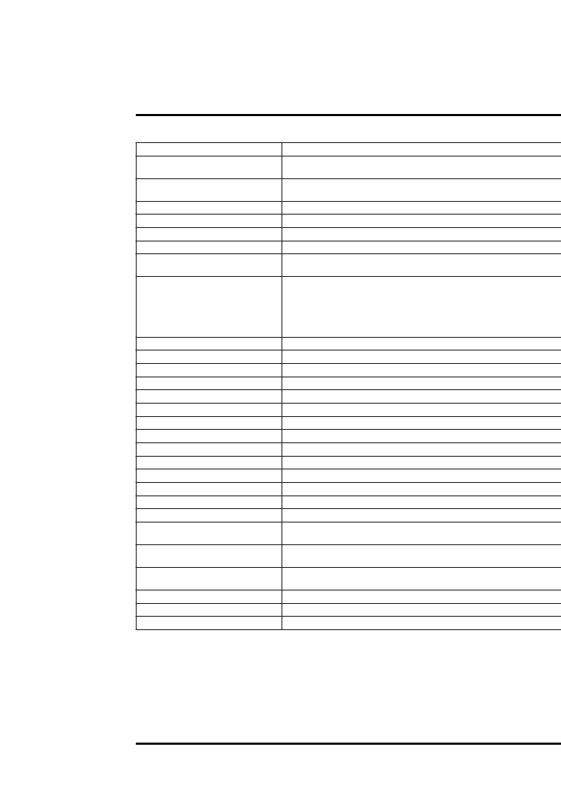
Signal Descriptions
Signal Names
Descriptions
TMS
Input – This pin is the Test Mode Select input, which is used to control the IEEE 1149.1
state machine.
Input – This pin is the Test Clock input pin, used to clock the IEEE 1149.1 state
machine.
Input – This pin is the IEEE 1149.1 Test Data in pin, used to load data.
Output – This pin is the IEEE 1149.1 Test Data out pin used to shift data out.
Input – Test Output Enable pin. TOE tristates all I/O pins when driven low.
Input – Global output enable inputs.
Input – This pin resets all the registers in the device. The global polarity (active high or
active low) for this pin is selectable on a global basis.
Input/Output – These are the general purpose I/O used by the logic array.
y
is the MFB
reference (alpha) and z is the macrocell reference (numeric)
y: A-X (768 macrocells)
y: A-P (512 macrocells)
y: A-H (256 macrocells)
z: 0-31
GND – Ground
No connect
V
CC
– The power supply pins for core logic.
V
CC
– The power supply pins for I/O banks 0, 1, 2, and 3.
Input – This pin de
fi
nes the reference voltage for I/O banks 0, 1, 2, and 3.
Input – Global clock/clock enable inputs (see Figure 14 for differential pairing).
Output – Optional clock output from PLL 0 and 1.
Input – Optional input resets the M divider in PLL 0 and 1.
Input – Optional feedback input for PLL 0 and 1.
GND – Ground for PLLs.
V
CC
– The power supply pin for PLLs.
V
CC
– The power supply for the IEEE 1149.1 interface.
I/O – sysCONFIG data pins, bit
x
.
Input – sysCONFIG interface chip select. Drive low to select sysCONFIG interface.
Input – De
fi
nes SRAM con
fi
guration mode. Low: sysCONFIG port, high: E
2
CMOS or
IEEE 1149.1 TAP.
Input – Controls the programming of SRAM. Hold high for normal operation. Toggle low
to reload SRAM from E
2
memory.
Input – Clock for sysCONFIG interface. Reads and writes occur on the rising edge of
the clock.
Input – Drive high to perform reads from the sysCONFIG interface.
I/O – Indicates status of con
fi
guration. Can be driven low to inhibit con
fi
guration.
Output (open drain) – Indicates status of con
fi
guration.
1. These inputs should not toggle during power up for proper power-up con
fi
guration.
TCK
TDI
TDO
TOE
GOE0, GOE1
RESET
yzz
GND
NC
V
CC
V
CCO0,
V
CCO1,
V
CCO2,
V
CCO3
V
REF0,
V
REF1,
V
REF2,
V
REF3
GCLK0, GCLK1, GCLK2, GCLK3
CLK_OUT0, CLK_OUT1
PLL_RST0, PLL_RST1
PLL_FBK0, PLL_FBK1
GNDP
V
CCP
V
CCJ
DATA
x
CSB
CFG0
PROGRAMB
CCLK
1
READ
1
INITB
DONE
相關(guān)PDF資料 |
PDF描述 |
|---|---|
| LC5256MC-5F256C | 3.3V, 2.5V and 1.8V In-System Programmable eXpanded Programmable Logic Device XPLD⑩ Family |
| LC5256MC-75F256C | 3.3V, 2.5V and 1.8V In-System Programmable eXpanded Programmable Logic Device XPLD⑩ Family |
| LC5512MC-45F256C | 3.3V, 2.5V and 1.8V In-System Programmable eXpanded Programmable Logic Device XPLD⑩ Family |
| LC5512MC-45F484C | 3.3V, 2.5V and 1.8V In-System Programmable eXpanded Programmable Logic Device XPLD⑩ Family |
| LC5512MC-45Q208C | 3.3V, 2.5V and 1.8V In-System Programmable eXpanded Programmable Logic Device XPLD⑩ Family |
相關(guān)代理商/技術(shù)參數(shù) |
參數(shù)描述 |
|---|---|
| LC5256MC-4F256I | 制造商:LATTICE 制造商全稱:Lattice Semiconductor 功能描述:3.3V, 2.5V and 1.8V In-System Programmable eXpanded Programmable Logic Device XPLD⑩ Family |
| LC5256MC-4F484C | 制造商:LATTICE 制造商全稱:Lattice Semiconductor 功能描述:3.3V, 2.5V and 1.8V In-System Programmable eXpanded Programmable Logic Device XPLD⑩ Family |
| LC5256MC-4F484I | 制造商:LATTICE 制造商全稱:Lattice Semiconductor 功能描述:3.3V, 2.5V and 1.8V In-System Programmable eXpanded Programmable Logic Device XPLD⑩ Family |
| LC5256MC-4F672C | 制造商:LATTICE 制造商全稱:Lattice Semiconductor 功能描述:3.3V, 2.5V and 1.8V In-System Programmable eXpanded Programmable Logic Device XPLD⑩ Family |
| LC5256MC-4F672I | 制造商:LATTICE 制造商全稱:Lattice Semiconductor 功能描述:3.3V, 2.5V and 1.8V In-System Programmable eXpanded Programmable Logic Device XPLD⑩ Family |
發(fā)布緊急采購(gòu),3分鐘左右您將得到回復(fù)。