- 您現(xiàn)在的位置:買賣IC網(wǎng) > PDF目錄30736 > LC78631E SPECIALTY CONSUMER CIRCUIT, PQFP80 PDF資料下載
參數(shù)資料
| 型號: | LC78631E |
| 元件分類: | 消費家電 |
| 英文描述: | SPECIALTY CONSUMER CIRCUIT, PQFP80 |
| 封裝: | QFP-80 |
| 文件頁數(shù): | 33/34頁 |
| 文件大小: | 502K |
| 代理商: | LC78631E |
第1頁第2頁第3頁第4頁第5頁第6頁第7頁第8頁第9頁第10頁第11頁第12頁第13頁第14頁第15頁第16頁第17頁第18頁第19頁第20頁第21頁第22頁第23頁第24頁第25頁第26頁第27頁第28頁第29頁第30頁第31頁第32頁當前第33頁第34頁

No. 5342-8/34
LC78631E
Pin Functions
Note:
Of the general-purpose I/O ports, any unused input ports must be connected to 0 V, or set to be output ports.
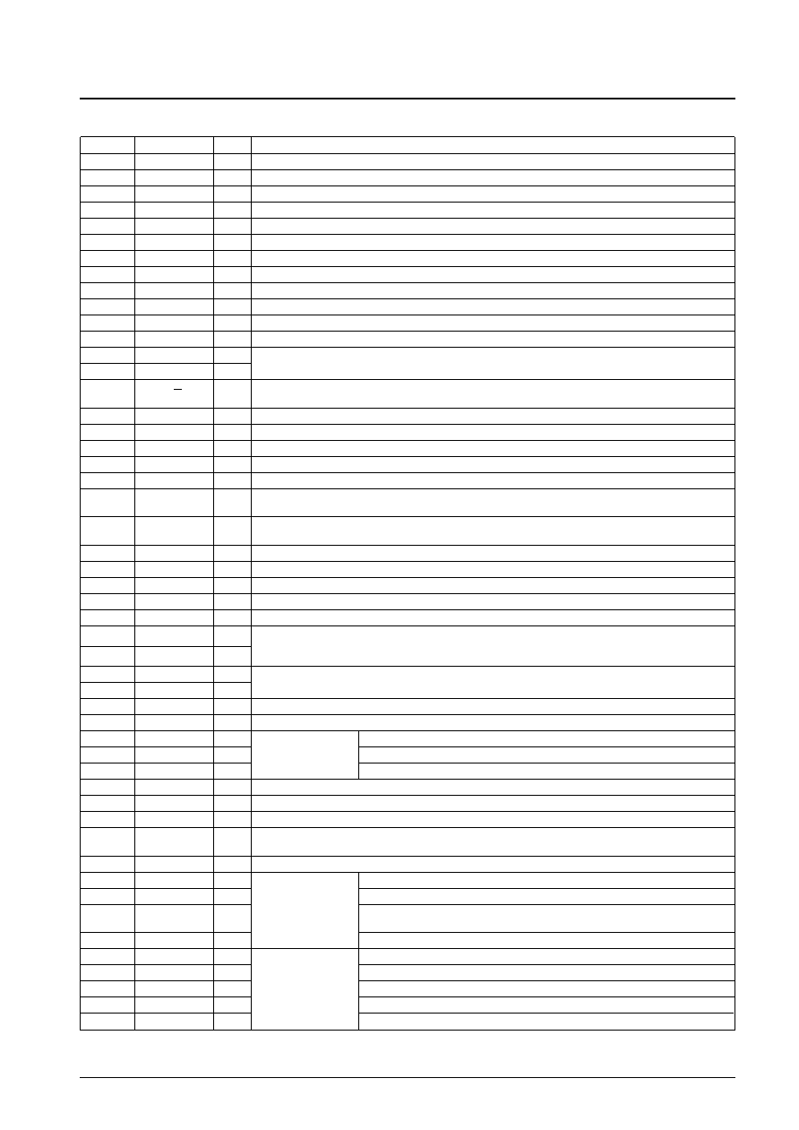
Pin No.
Symbol
I/O
Function
1
VPDO
O
Variable pitch PLL charge pump output. Must be left open if unused.
2
PDO2
O
Double-speed and quad-speed mode playback PLL charge pump output. Must be left open if unused.
3
PDO1
O
Normal-speed mode playback PLL charge pump output
4
AVSS
Analog system ground. Must be connected to 0 V.
5
FR
Built-in VCO frequency range setting resistor connection
6
AVDD
Analog system power supply
7
ISET
PDO1 and PDO2 output current setting resistor connection
8
TAI
I
Test input. A pull-down resistor is built in. Must be connected to 0 V.
9
EFMO
O
EFM signal output
10
VSS
Digital system ground. Must be connected to 0 V.
11
EFMI
I
EFM signal input
12
TEST1
I
Test input. A pull-down resistor is built in. Must be connected to 0 V.
13
CLV+
O
Spindle servo control output. CLV+ outputs a high level for acceleration, and CLV– outputs a high level for
14
CLV–
O
deceleration.
15
V/P
O
Rough servo/phase control automatic switching monitor output. A high-level output indicates rough servo, and a
low-level output indicates phase control.
16
TEST2
I
Test input. A pull-down resistor is built in. Must be connected to 0 V.
17
TEST3
I
Test input. A pull-down resistor is built in. Must be connected to 0 V.
18
P4
I/O
I/O port
19
HFL
I
Track detection signal input. This is a Schmitt input.
20
TES
I
Tracking error signal input. This is a Schmitt input.
21
PCK
O
EFM data playback bit clock monitor. Outputs 4.3218 MHz when the phase is locked in normal-speed mode
playback.
22
FSEQ
O
Synchronization signal detection output. Outputs a high level when the synchronization signal detected from the
EFM signal matches the internally generated synchronization signal.
23
TOFF
O
Tracking off output
24
TGL
O
Tracking gain switching output. Increase the gain when this pin outputs a low level.
25
THLD
O
Tracking hold output
26
TEST4
I
Test input. A pull-down resistor is built in. Must be connected to 0 V.
27
VDD
Digital system power supply
28
JP+
O
Track jump output. JP+ outputs a high level both for acceleration during outward direction jumps and for
deceleration during inward direction jumps. JP– outputs a high level both for acceleration during inward direction
29
JP–
O
jumps and for deceleration during outward direction jumps.
30
SLD+
O
Sled output. This pin can be set to 1 of 4 levels by commands sent from the system control microprocessor.
31
SLD–
O
32
EMPH
O
De-emphasis monitor. A high level indicates that a disk requiring de-emphasis is being played.
33
P5
I/O
I/O port
34
LRCKO
O
LR clock output
35
DFLRO
O
Digital filter outputs
LR data output. The digital filter can be turned off with the DFOFF command.
36
DACKO
O
Bit clock output
37
CONT1
O
Output port
38
P0/DFCK
I/O
I/O port. DF bit clock input in antishock mode.
39
P1/DFIN
I/O
I/O port. DF data input in antishock mode.
40
P2
I/O
I/O port. Used as the de-emphasis filter on/off switching pin in antishock mode. The de-emphasis filter is turned
on when this pin is high.
41
P3/DFLR
I/O
I/O port output or digital filter LR clock input (when anti-shock mode)
42
LRSY
O
LR clock output
43
CK2
O
Bit clock output. The polarity can be inverted with the CK2CON command.
44
ROMXA
O
ROMXA pins
Interpolated data output. Data that has not been interpolated can be output by issuing
the ROMXA command.
45
C2F
O
C2 flag output
46
MUTEL
O
Left channel mute output
47
LVDD
Left channel power supply
48
LCHP
O
One-bit D/A
Left channel P output
49
LCHN
O
converter pins
Left channel N output
50
LVSS
Left channel ground. Must be connected to 0V.
Continued on next page.
相關PDF資料 |
PDF描述 |
|---|---|
| LC78637E | SPECIALTY CONSUMER CIRCUIT, PQFP80 |
| LC78647NT | SPECIALTY CONSUMER CIRCUIT, PQFP100 |
| LC78648E | SPECIALTY CONSUMER CIRCUIT, PQFP80 |
| LC78681E | SPECIALTY CONSUMER CIRCUIT, PQFP64 |
| LC78681KE-L | SPECIALTY CONSUMER CIRCUIT, PQFP64 |
相關代理商/技術參數(shù) |
參數(shù)描述 |
|---|---|
| LC78632 | 制造商:SANYO 制造商全稱:Sanyo Semicon Device 功能描述:Compact Disk Player DSP |
| LC78632RE | 制造商:SANYO 制造商全稱:Sanyo Semicon Device 功能描述:Compact Disk Player DSP |
| LC78637E-E | 制造商:ON Semiconductor 功能描述: |
| LC7863KA | 制造商:未知廠家 制造商全稱:未知廠家 功能描述: |
| LC78641E | 制造商:未知廠家 制造商全稱:未知廠家 功能描述:CD-Player Processor/Controller |
發(fā)布緊急采購,3分鐘左右您將得到回復。