- 您現(xiàn)在的位置:買賣IC網(wǎng) > PDF目錄4585 > LFXP6C-5F256C (Lattice Semiconductor Corporation)IC FPGA 5.8KLUTS 188I/O 256-BGA PDF資料下載
參數(shù)資料
| 型號: | LFXP6C-5F256C |
| 廠商: | Lattice Semiconductor Corporation |
| 文件頁數(shù): | 140/397頁 |
| 文件大小: | 0K |
| 描述: | IC FPGA 5.8KLUTS 188I/O 256-BGA |
| 標(biāo)準(zhǔn)包裝: | 90 |
| 系列: | XP |
| 邏輯元件/單元數(shù): | 6000 |
| RAM 位總計(jì): | 73728 |
| 輸入/輸出數(shù): | 188 |
| 電源電壓: | 1.71 V ~ 3.465 V |
| 安裝類型: | 表面貼裝 |
| 工作溫度: | 0°C ~ 85°C |
| 封裝/外殼: | 256-BGA |
| 供應(yīng)商設(shè)備封裝: | 256-FPBGA(17x17) |
LatticeECP/EC and LatticeXP
Lattice Semiconductor
DDR Usage Guide
10-5
DDR Software Primitives
This section describes the software primitives that can be used to implement DDR interfaces and provides details
about how to instantiate them in the software. The primitives described include:
DQSDLL
The DQS delay calibration DLL
DQSBUF
The DQS delay function and the clock polarity selection logic
INDDRXB The DDR input and DQS to system clock transfer registers
ODDRXB
The DDR output registers
An HDL usage example for each of these primitives is listed in Appendices B and C.
DQSDLL
The DQSDLL will generate a 90-degree phase shift required for the DQS signal. This primitive will implement the
on-chip DQSDLL. Only one DQSDLL should be instantiated for all the DDR implementations on one half of the
device. The clock input to this DLL should be at the same frequency as the DDR interface. The DLL will generate
the delay based on this clock frequency and the update control input to this block. The DLL will update the dynamic
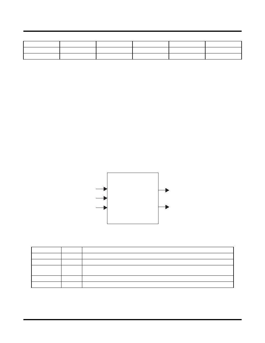
delay control to the DQS delay block when this update control (UDDCNTL) input is asserted. Figure 10-5 shows
the primitive symbol. The active low signal on UDDCNTL updates the DQS phase alignment and should be initi-
ated at the beginning of READ cycles.
Figure 10-5. DQSDLL Symbol
Table 10-4 provides a description of the ports.
Table 10-4. DQSDLL Ports
DQSDLL Configuration Attributes
By default this DLL will generate a 90-degree phase shift for the DQS strobe based on the frequency of the input
reference clock to the DLL. The user can control the sensitivity to jitter by using the LOCK_SENSITIVITY attribute.
This configuration bit can be programmed to be either “HIGH” or “LOW”.
PL11B
7
C
—
H6
J5
PL12A
7
T
—
G3
K4
Port Name
I/O
Definition
CLK
I
System CLK should be at frequency of the DDR interface, from the FPGA core.
RST
I
Resets the DQSDLL
UDDCNTL
I
Provides an update signal to the DLL that will update the dynamic delay. When held low
this signal will update the DQSDEL.
LOCK
O
Indicates when the DLL is in phase
DQSDEL
O
The digital delay generated by the DLL should be connected to the DQSBUF primitive.
Table 10-3. EC20 Pinout (from LatticeECP/EC Family Data Sheet)
Ball Function
Bank
LVDS
Dual Function
484 fpBGA
672 fpBGA
CLK
RST
UDDCNTL
LOCK
DQSDEL
DQSDLL
相關(guān)PDF資料 |
PDF描述 |
|---|---|
| HSC49DRTN-S93 | CONN EDGECARD 98POS DIP .100 SLD |
| LFXP6C-4FN256I | IC FPGA 5.8KLUTS 188I/O 256-BGA |
| HSC49DRTH-S93 | CONN EDGECARD 98POS DIP .100 SLD |
| HSC49DREN-S93 | CONN EDGECARD 98POS .100 EYELET |
| IDT89HPES16NT2ZBBC | IC PCI SW 16LANE 2PORT 484-CABGA |
相關(guān)代理商/技術(shù)參數(shù) |
參數(shù)描述 |
|---|---|
| LFXP6C-5FN256C | 功能描述:FPGA - 現(xiàn)場可編程門陣列 5.8K LUTS 188 I/O RoHS:否 制造商:Altera Corporation 系列:Cyclone V E 柵極數(shù)量: 邏輯塊數(shù)量:943 內(nèi)嵌式塊RAM - EBR:1956 kbit 輸入/輸出端數(shù)量:128 最大工作頻率:800 MHz 工作電源電壓:1.1 V 最大工作溫度:+ 70 C 安裝風(fēng)格:SMD/SMT 封裝 / 箱體:FBGA-256 |
| LFXP6C-5Q208C | 功能描述:FPGA - 現(xiàn)場可編程門陣列 5.8K LUTs 142 IO 1.8 /2.5/3.3V -5 Spd RoHS:否 制造商:Altera Corporation 系列:Cyclone V E 柵極數(shù)量: 邏輯塊數(shù)量:943 內(nèi)嵌式塊RAM - EBR:1956 kbit 輸入/輸出端數(shù)量:128 最大工作頻率:800 MHz 工作電源電壓:1.1 V 最大工作溫度:+ 70 C 安裝風(fēng)格:SMD/SMT 封裝 / 箱體:FBGA-256 |
| LFXP6C-5QN208C | 功能描述:FPGA - 現(xiàn)場可編程門陣列 5.8K LUTS 142 I/O RoHS:否 制造商:Altera Corporation 系列:Cyclone V E 柵極數(shù)量: 邏輯塊數(shù)量:943 內(nèi)嵌式塊RAM - EBR:1956 kbit 輸入/輸出端數(shù)量:128 最大工作頻率:800 MHz 工作電源電壓:1.1 V 最大工作溫度:+ 70 C 安裝風(fēng)格:SMD/SMT 封裝 / 箱體:FBGA-256 |
| LFXP6-C-5T144C | 制造商:Lattice Semiconductor 功能描述:FPGA LatticeXP Family 6000 Cells 400MHz 130nm (CMOS) Technology 1.8V/2.5V/3.3V 144-Pin TQFP Tray |
| LFXP6C-5T144C | 功能描述:FPGA - 現(xiàn)場可編程門陣列 5.8K LUTs 100 IO 1.8 /2.5/3.3V -5 Spd RoHS:否 制造商:Altera Corporation 系列:Cyclone V E 柵極數(shù)量: 邏輯塊數(shù)量:943 內(nèi)嵌式塊RAM - EBR:1956 kbit 輸入/輸出端數(shù)量:128 最大工作頻率:800 MHz 工作電源電壓:1.1 V 最大工作溫度:+ 70 C 安裝風(fēng)格:SMD/SMT 封裝 / 箱體:FBGA-256 |
發(fā)布緊急采購,3分鐘左右您將得到回復(fù)。