- 您現(xiàn)在的位置:買賣IC網 > PDF目錄358799 > LH6V4256 (Sharp Corporation) CMOS 1M (256K x 4) Dynamic RAM PDF資料下載
參數(shù)資料
| 型號: | LH6V4256 |
| 廠商: | Sharp Corporation |
| 英文描述: | CMOS 1M (256K x 4) Dynamic RAM |
| 中文描述: | 100萬的CMOS(256K × 4)動態(tài)隨機存儲器 |
| 文件頁數(shù): | 6/18頁 |
| 文件大小: | 198K |
| 代理商: | LH6V4256 |

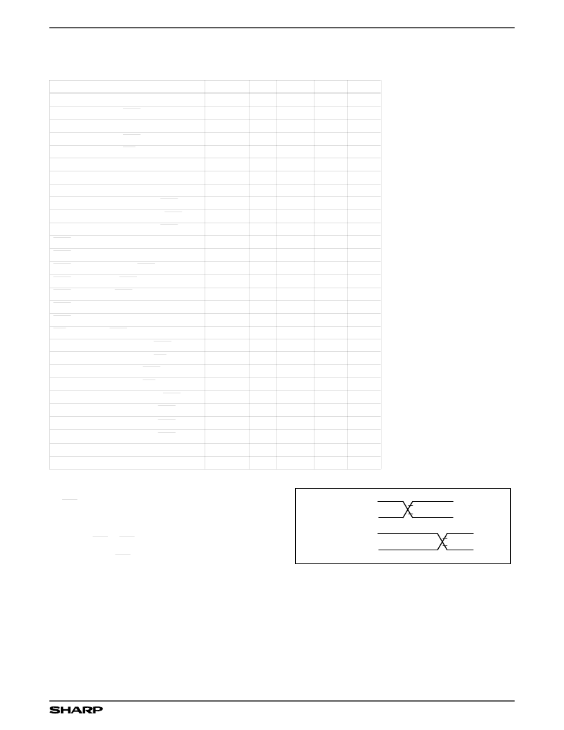
AC ELECTRICAL CHARACTERISTICS
1, 2, 3, 4
(T
A
= 0 to +70
°
C, V
CC
= 3.3 V
±
0.3 V)
READ CYCLE
PARAMETER
SYMBOL
MIN.
MAX.
UNIT
NOTE
Random read or write cycle time
Access time from RAS
Access time from column address
Access time from CAS
Access time from OE
Row address setup time
Row address hold time
Column address setup time
Column address hold time (RAS)
Column address delay time (RAS)
Column address lead time (RAS)
RAS pulse width
RAS precharge time
CAS precharge time (RAS
↓
)
CAS delay time (RAS)
CAS lead time (RAS)
CAS pulse width
CAS hold time
OE lead time (RAS)
Output data disable time (CAS)
Output data disable time (OE)
Output data hold time (CAS)
Output data hold time (OE)
Read command setup time (CAS)
Read command hold time (CAS)
Read command hold time (RAS
↑
)
Read command hold time (RAS
↓
)
Transition time (rise and fall)
Refresh time interval
t
RC
t
RAC
t
AA
t
CAC
t
OEA
t
ASR
t
RAH
t
ASC
t
CAH
t
RAD
t
RAL
t
RAS
t
RP
t
CRP
t
RCD
t
RSL
t
CAS
t
CSH
t
ROL
t
OFF
t
OEZ
t
SOH
t
OOH
t
RCS
t
RCH
t
RRHP
t
RRHN
t
T
t
REF
190
ns
ns
ns
ns
ns
ns
ns
ns
ns
ns
ns
ns
ns
ns
ns
ns
ns
ns
ns
ns
ns
ns
ns
ns
ns
ns
ns
ns
ms
100
50
40
35
5
5
5
5
0
15
0
20
20
50
100
80
0
25
30
40
100
0
50
6
10,000
60
7
10,000
30
30
0
0
0
10
10
115
3
8
8
8
35
8
NOTES:
1.
For proper memory function, at least 200
μ
s of pause time should
be kept after power on, followed by several dummy cycles. When
RAS = V
is continued for more than 8 ms, the same dummy cycles
should be given. Usually eight ordinary refresh cycles should be
given.
2.
The required V
CC
current (I
CC
) during power on depends on the input
levels of RAS. If RAS = V
during power on, the device goes into
an active cycle, and I
exhibits large current transients. It is rec-
ommended that RAS tracks with V
CC
or be held at a valid V
IH
during
power on.
3.
AC characteristics assume t
T
= 5 ns.
4.
AC characteristics assume the following condition (see figure at
right).
5.
Load condition for 1TTL + 30 pF.
6.
t
RAD
(MAX) is the maximum point for t
RAD
where t
RAC
(MAX) is
ensured, and does not represent a limit of operation. If t
RAD
≥
t
RAD
(MAX), the access time comes under the control of t
AA
.
7.
t
RCD
(MAX) is the maximum point for t
RCD
, where t
RAC
(MAX) is
ensured and does not represent a limit of operation. If t
RCD
≥
t
RCD
(MAX), the access time comes under the control of t
CAC
.
8.
The operation is ensured when either t
RRHN
, t
RRHP
, or t
RCH
is satisfied.
6V4256-6
INPUT
LEVEL
2.3 V
0.6 V
2.15 V
0.4 V
OUTPUT
JUDGMENT
LEVEL
CMOS 1M (256K
×
4) Dynamic RAM
LH6V4256
2-19
相關PDF資料 |
PDF描述 |
|---|---|
| LH75400 | System-on-Chip |
| LH77790B | Embedded Microcontroller(32位嵌入式微控制器) |
| LH79525 | 16/32-bit System-on-Chip with Color LCD Controller |
| LH7A400 | 32-Bit System-on-Chip |
| LH7A400N0B000 | 32-Bit System-on-Chip |
相關代理商/技術參數(shù) |
參數(shù)描述 |
|---|---|
| LH6V4256D-10 | 制造商:未知廠家 制造商全稱:未知廠家 功能描述:x4 Fast Page Mode DRAM |
| LH6V4256K-10 | 制造商:未知廠家 制造商全稱:未知廠家 功能描述:x4 Fast Page Mode DRAM |
| LH6V4256T-10 | 制造商:未知廠家 制造商全稱:未知廠家 功能描述:x4 Fast Page Mode DRAM |
| LH7001 | 制造商:NSC 制造商全稱:National Semiconductor 功能描述:POSITIVE / NEGATIVE ADJUSTABLE REGULATOR |
| LH7001CN | 制造商:NSC 制造商全稱:National Semiconductor 功能描述:POSITIVE / NEGATIVE ADJUSTABLE REGULATOR |
發(fā)布緊急采購,3分鐘左右您將得到回復。