- 您現(xiàn)在的位置:買賣IC網(wǎng) > PDF目錄361025 > LM2744 (National Semiconductor Corporation) Low Voltage N-Channel MOSFET Synchronous Buck Regulator Controller with External Reference PDF資料下載
參數(shù)資料
| 型號: | LM2744 |
| 廠商: | National Semiconductor Corporation |
| 英文描述: | Low Voltage N-Channel MOSFET Synchronous Buck Regulator Controller with External Reference |
| 中文描述: | 低壓N溝道MOSFET同步降壓穩(wěn)壓控制器與外部參考 |
| 文件頁數(shù): | 2/22頁 |
| 文件大小: | 663K |
| 代理商: | LM2744 |
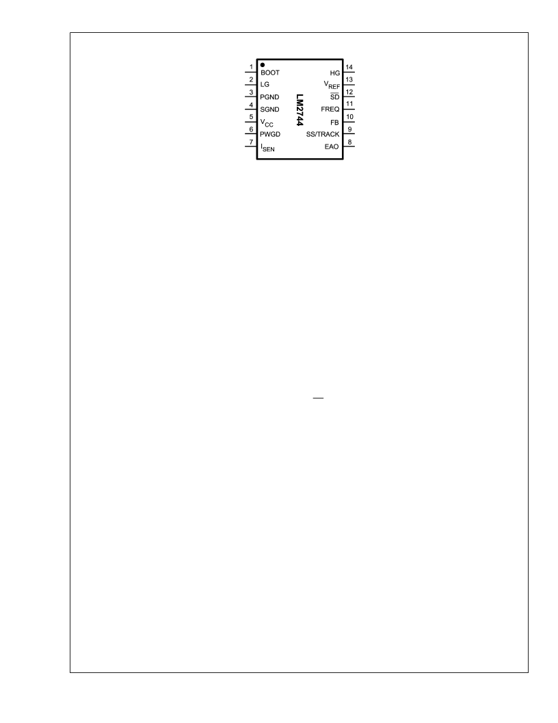
Connection Diagram
20106002
14-Lead Plastic TSSOP
θ
= 155C/W
NS Package Number MTC14
Pin Description
BOOT (Pin 1)
- Bootstrap pin. This is the supply rail for the
high-side gate driver. When the high-side MOSFET turns on,
the voltage on this pin should be at least one gate threshold
above the regulator input voltage V
IN
to properly turn on the
MOSFET. See MOSFET Gate Drivers in the Application
Information section for more details on how to select MOS-
FETs.
LG (Pin 2)
- Low-gate drive pin. This is the gate drive for the
low-side N-channel MOSFET. This signal is interlocked with
the high-side gate drive HG (Pin 14), so as to avoid shoot-
through.
PGND (Pin 3)
- Power ground. This is also the ground for the
low-side MOSFET driver. This pin must be connected on the
PCB ground plane, which is usually also the system ground.
SGND (Pin 4)
- Signal ground. It should be connected
appropriately to the ground plane with due regard to good
layout practices in switching power regulator circuits.
V
CC
(Pin 5)
Supply rail for the control sections of the IC.
PWGD (Pin 6)
- Power Good pin. This is an open drain
output, which is typically meant to be connected to V
or
any other low voltage source through a pull-up resistor. The
voltage on this pin is thus pulled low under output fault
conditions (undervoltage or overvoltage) and also under
UVLO.
I
SEN
(Pin 7)
- Current limit threshold setting pin. This sources
a fixed 40 μA current. A resistor of appropriate value should
be connected between this pin and the drain of the low-side
MOSFET (switch node).
EAO (Pin 8)
- Output of the error amplifier. The voltage level
on this pin is compared with an internally generated ramp
signal to determine the duty cycle. This pin is necessary for
compensating the control loop.
SS/TRACK (Pin 9)
- Soft-start and tracking pin. This pin is
internally connected to the non-inverting input of the error
amplifier during soft-start, and in fact any time the SS/
TRACK pin voltage happens to be below the internal refer-
ence voltage. For the basic soft-start function, a capacitor of
minimum value 1nF is connected from this pin to ground. To
track the rising ramp of another power supply’s output, con-
nect a resistor divider from the output of that supply to this
pin as described in Application Information.
FB (Pin 10)
- Feedback pin. This is the inverting input of the
error amplifier, which is used for sensing the output voltage
and compensating the control loop.
FREQ (Pin 11)
- Frequency adjust pin. The switching fre-
quency is set by connecting a resistor of suitable value
between this pin and ground. The equation for calculating
the exact value is provided in Application Information, but
some typical values (rounded up to the nearest standard
values) are 324 k
for 100 kHz, 97.6 k
for 300 kHz, 56.2
k
for 500 kHz, 24.9 k
for 1 MHz.
SD (Pin 12)
- IC shutdown pin. Pull this pin to V
to ensure
the IC is enabled. Connect to ground to disable the IC. Under
shutdown, both high-side and low-side drives are off. This
pin also features a precision threshold for power supply
sequencing purposes, as well as a low threshold to ensure
minimal quiescent current.
V
REF
(Pin 13)
- External reference. This goes to the non-
inverting input of the error amplifier. Any desired reference
voltage between 0.5V to 1.5V can be connected to this pin
(with appropriate filtering if necessary).
HG (Pin 14)
- High-gate drive pin. This is the gate drive for
the high-side N-channel MOSFET. This signal is interlocked
with LG (Pin 2) to avoid shoot-through.
L
www.national.com
2
相關(guān)PDF資料 |
PDF描述 |
|---|---|
| LM2796TL | Dual-Display White LED Driver with 3/2x Switched Capacitor Boost |
| LM2796TLX | Dual-Display White LED Driver with 3/2x Switched Capacitor Boost |
| LM2796 | Dual-Display White LED Driver with 3/2x Switched Capacitor Boost |
| LM2925 | Cap-Free, NMOS, 150mA Low Dropout Regulator with Reverse Current Protection |
| LM2925T | Cap-Free, NMOS, 150mA Low Dropout Regulator with Reverse Current Protection |
相關(guān)代理商/技術(shù)參數(shù) |
參數(shù)描述 |
|---|---|
| LM2744EVAL | 功能描述:電源管理IC開發(fā)工具 EVAL BOARD RoHS:否 制造商:Maxim Integrated 產(chǎn)品:Evaluation Kits 類型:Battery Management 工具用于評估:MAX17710GB 輸入電壓: 輸出電壓:1.8 V |
| LM2744MTC | 功能描述:DC/DC 開關(guān)控制器 RoHS:否 制造商:Texas Instruments 輸入電壓:6 V to 100 V 開關(guān)頻率: 輸出電壓:1.215 V to 80 V 輸出電流:3.5 A 輸出端數(shù)量:1 最大工作溫度:+ 125 C 安裝風(fēng)格: 封裝 / 箱體:CPAK |
| LM2744MTC/NOPB | 功能描述:DC/DC 開關(guān)控制器 RoHS:否 制造商:Texas Instruments 輸入電壓:6 V to 100 V 開關(guān)頻率: 輸出電壓:1.215 V to 80 V 輸出電流:3.5 A 輸出端數(shù)量:1 最大工作溫度:+ 125 C 安裝風(fēng)格: 封裝 / 箱體:CPAK |
| LM2744MTCX | 功能描述:DC/DC 開關(guān)控制器 RoHS:否 制造商:Texas Instruments 輸入電壓:6 V to 100 V 開關(guān)頻率: 輸出電壓:1.215 V to 80 V 輸出電流:3.5 A 輸出端數(shù)量:1 最大工作溫度:+ 125 C 安裝風(fēng)格: 封裝 / 箱體:CPAK |
| LM2744MTCX/NOPB | 功能描述:DC/DC 開關(guān)控制器 RoHS:否 制造商:Texas Instruments 輸入電壓:6 V to 100 V 開關(guān)頻率: 輸出電壓:1.215 V to 80 V 輸出電流:3.5 A 輸出端數(shù)量:1 最大工作溫度:+ 125 C 安裝風(fēng)格: 封裝 / 箱體:CPAK |
發(fā)布緊急采購,3分鐘左右您將得到回復(fù)。