- 您現(xiàn)在的位置:買賣IC網(wǎng) > PDF目錄361025 > LM3075MTCX (NATIONAL SEMICONDUCTOR CORP) High Efficiency, Synchronous Current Mode Buck Controller PDF資料下載
參數(shù)資料
| 型號: | LM3075MTCX |
| 廠商: | NATIONAL SEMICONDUCTOR CORP |
| 元件分類: | 穩(wěn)壓器 |
| 英文描述: | High Efficiency, Synchronous Current Mode Buck Controller |
| 中文描述: | SWITCHING CONTROLLER, 330 kHz SWITCHING FREQ-MAX, PDSO20 |
| 封裝: | TSSOP-20 |
| 文件頁數(shù): | 12/18頁 |
| 文件大?。?/td> | 857K |
| 代理商: | LM3075MTCX |
Operating Descriptions
(Continued)
level of 2V (typical) and it enters ready mode as it does when
the IC first was powered up. The UVP stays in ready mode
until a new under-voltage event is detected.
POWER GOOD FUNCTION
A power good signal is available for indicating the general
state of the IC. The function is realized through the internal
MOSFET tied from the PGOOD pin to ground. The power
good signal is asserted by turning off the MOSFET. The on
resistance of the power good MOSFET is about 300
. The
internal power good MOSFET is not turned on unless at
least one of the following occurs:
1.
There is an output over-voltage event.
2.
The output voltage is below the power good lower limit
(UVP event).
3.
System is in shutdown mode, i.e. the EN pin voltage is
below 0.6V.
As with the other protection responses, the power good
signal has built-in hysteresis. See V
PWR_GOOD
in the Elec-
trical Characteristics table.
FREQUENCY SELECT
The operating frequency may be set at 200 kHz or 300 kHz
by the voltage on the frequency select (FS) pin. A voltage of
0V corresponds to a frequency of 200 kHz and a voltage of
5V corresponds to a frequency of 300 kHz. See the Electrical
Characteristics table for more information.
VLIN5, VDD and EXT
An internal 5V supply (V
LIN5
) is generated from the V
IN
voltage through an internal linear regulator. This 5V supply is
mainly for internal circuitry use, but can also be used exter-
nally. When used externally, it is recommended that the
V
voltage only be used for powering the gate drivers, i.e.
supplying the bias for the top drivers’ bootstrap circuit and
the bottom drivers’ VDD pins. When the voltage applied to
the EXT pin is below 4.7V, an internal 5V low dropout regu-
lator supplies the power for the V
. If the EXT voltage is
taken above 4.7V, the 5V regulator is turned off and an
internal switch is turned on to connect the EXT pin to the
VLIN5 pin. This allows the VLIN5 power to be derived from a
high efficiency source such as the output of the switching
channel, when the channel is configured to operate in fixed
5V mode. The V
voltage output comes from the EXT pin
whenever the voltage applied to the EXT pin is higher than
4.7V. The externally applied voltage is required to be less
than the voltage applied to the VIN pin at all times. This
prevents a voltage feedback situation from the EXT pin to
the VIN pin. When the input voltage must be guaranteed to
be within 4.5V to 5.5V, tie the VLIN5 pin directly to the VIN
pin and tie the EXT pin to ground. In this mode, the V
LIN5
current directly comes from power stage input rail and power
loss due to the internal linear regulation is no longer an
issue. Always connect the VDD pin to the VLIN5 pin through
a 4.7
resistor and connect a ceramic capacitor of at least 1
μF to bypass the VDD pin to ground.
THERMAL PROTECTION
The LM3075 IC enters thermal protection mode if the die
temperature exceeds 160C. In this mode, the top and bot-
tom FETs are turned off immediately. The IC then behaves in
a manner as described in the
Fault State
section.
OUTPUT CAPACITORS FOR LINEAR REGULATORS
Like any linear regulator, the linear output that is either
generated or controlled by the LM3075 requires an output
capacitor to ensure stability. The output of VLIN5 needs a
minimum of 4.7 μF.
SWITCHING NOISE REDUCTION
Power MOSFETs are very fast switching devices. In a syn-
chronous rectifier converter, the rapid drain current rise rate
of the top FET coupled with parasitic inductance generates
unwanted Ldi/dt spike noise at the source node of the FET
(SW pin). The magnitude of the spike noise increases as the
output current increases. This parasitic spike noise may turn
into electromagnetic interference (EMI) that may cause
trouble to the system performance. Therefore, it is vital to
correct system performance to suppress this kind of noise.
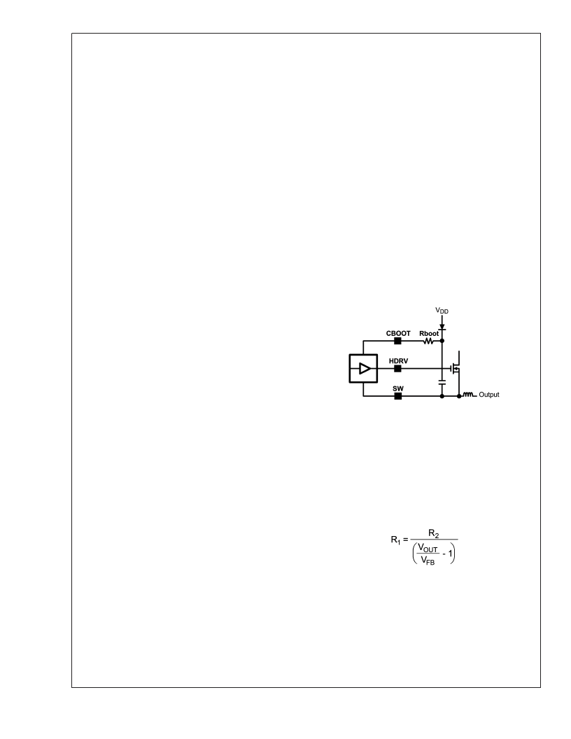
As shown in Figure 3, adding a resistor in series with the
CBOOT pin scales the spikes and slow down the gate drive
(HDRV) rise time of the top FET to yield a desired drain
current transition time. Usually a 3.3
to 5.1
resistor is
sufficient to suppress the noise. It is important to note that
the addition of these resistors does increase the power loss
in the system and thus decreases the efficiency. It is there-
fore important to choose the size of the resistor carefully; the
top FET switching losses increases with higher resistance
values.
Component Selection
OUTPUT VOLTAGE SETTING
The output voltage for each channel is set by the ratio of a
voltage divider as shown in
Figure 4
. The resistor values can
be determined by the following equation:
(1)
Where V
is the typical value of feedback pin voltage and
V
is the nominal output voltage . Although increasing the
value of R
and R
increases efficiency, this also decreases
accuracy. Therefore, a maximum value is recommended for
R
in order to keep the output within 0.3% of V
. This
maximum R
2
value should be calculated first with the follow-
ing equation:
20162310
FIGURE 3. Adding a resistor in series with the CBOOT
pin to suppress the turn-on switching noise
L
www.national.com
12
相關(guān)PDF資料 |
PDF描述 |
|---|---|
| LM3080 | Operational Transconductance Amplifier |
| LM3080AN | Operational Transconductance Amplifier |
| LM3080M | CAP 16V 470UF SOLID ELECT AXIAL |
| LM3080N | Operational Transconductance Amplifier |
| LM3086 | LM3045/LM3046/LM3086 Transistor Arrays |
相關(guān)代理商/技術(shù)參數(shù) |
參數(shù)描述 |
|---|---|
| LM3075N/A+ | 制造商:未知廠家 制造商全稱:未知廠家 功能描述:FM Receiver Circuit |
| LM3075N/B+ | 制造商:未知廠家 制造商全稱:未知廠家 功能描述:FM Receiver Circuit |
| LM3075N-01/A+ | 制造商:未知廠家 制造商全稱:未知廠家 功能描述:FM Receiver Circuit |
| LM3075N-01/B+ | 制造商:未知廠家 制造商全稱:未知廠家 功能描述:FM Receiver Circuit |
| LM307AH | 制造商:Texas Instruments 功能描述: |
發(fā)布緊急采購,3分鐘左右您將得到回復(fù)。