- 您現(xiàn)在的位置:買賣IC網(wǎng) > PDF目錄361025 > LM3075MTCX (NATIONAL SEMICONDUCTOR CORP) High Efficiency, Synchronous Current Mode Buck Controller PDF資料下載
參數(shù)資料
| 型號: | LM3075MTCX |
| 廠商: | NATIONAL SEMICONDUCTOR CORP |
| 元件分類: | 穩(wěn)壓器 |
| 英文描述: | High Efficiency, Synchronous Current Mode Buck Controller |
| 中文描述: | SWITCHING CONTROLLER, 330 kHz SWITCHING FREQ-MAX, PDSO20 |
| 封裝: | TSSOP-20 |
| 文件頁數(shù): | 13/18頁 |
| 文件大小: | 857K |
| 代理商: | LM3075MTCX |
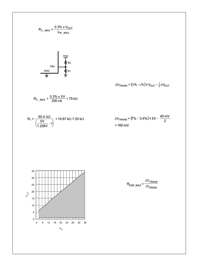
Component Selection
(Continued)
(2)
Where I
FB_MAX
is the maximum current drawn by the FB pin.
Example: V
OUT
= 5V, V
FB
= 1.238V, I
FB_MAX
= 200 nA.
(3)
R
2
is chosen to be 60.4 k
±
1%. To calculate R1:
(4)
The output voltage is limited by the maximum duty cycle as
well as the minimum on time. Figure 5 shows the limits for
input and output voltages. The recommended maximum out-
put voltage is approximately 1V less than the nominal input
voltage. At 30V input, the minimum output is approximately
2.3V and the maximum is approximately 27V. For input
voltages below 5.5V, VLIN5 must be connected to VIN
through a small resistor (approximately 4.7
). Doing this
ensures that VLIN5 does not fall below the UVLO threshold.
Output Capacitor Selection
In applications that exhibit large and fast load current
swings, the slew rate of such a load current transient may be
beyond the response speed of the regulator. Therefore, to
meet voltage transient requirements during worst-case load
transients, special consideration should be given to output
capacitor selection. The total combined ESR of the output
capacitors must be lower than a certain value, while the total
capacitance must be greater than a certain value. Also, in
applications where the specification of output voltage regu-
lation is tight and ripple voltage must be low, starting from the
required output voltage ripple (
V
OUT
) often results in fewer
design iterations.
ALLOWED TRANSIENT VOLTAGE EXCURSION
The allowed output voltage excursion during a load transient
(
V
TRANS
) is:
(5)
Where
δ
% is the output voltage regulation window,
e
% is the
output voltage initial accuracy V
is the nominal output
voltage, and
V
OUT
is the output voltage ripple.
Example: V
= 5V,
δ
% = 7%,
e
% = 3.4%,
V
OUT
= 40 mV
peak-to-peak.
(6)
Since the ripple voltage is included in the calculation of
V
TRANS
, the inductor ripple current should not be included
in the worst-case load current excursion. That is, the worst-
case load current excursion should be simply maximum load
current change specification,
I
TRANS
.
MAXIMUM ESR CALCULATION
Unless the rise and fall times of a load transient are slower
than the response speed of the control loop, if the total
combined ESR (R
) is too high, the load transient require-
ment is not met, no matter how large the capacitance. The
maximum allowed total combined ESR is:
(7)
Example:
V
TRANS
= 160mV,
I
TRANS
= 3A. Then R
esr_max
=
53.3m
.
Maximum ESR criterion can be used when the associated
capacitance is high enough, otherwise more capacitors than
the number determined by this criterion should be used in
parallel.
MINIMUM CAPACITANCE CALCULATION
In a switch mode power supply, the minimum output capaci-
tance is typically dictated by the load transient requirement.
If there is not enough capacitance, the output voltage excur-
sion will exceed the maximum allowed value even if the
maximum ESR requirement is met. The worst-case load
transient is an unloading transient that happens when the
20162312
FIGURE 4. Output Voltage Setting
20162314
FIGURE 5. Available Output Voltage Range
L
www.national.com
13
相關(guān)PDF資料 |
PDF描述 |
|---|---|
| LM3080 | Operational Transconductance Amplifier |
| LM3080AN | Operational Transconductance Amplifier |
| LM3080M | CAP 16V 470UF SOLID ELECT AXIAL |
| LM3080N | Operational Transconductance Amplifier |
| LM3086 | LM3045/LM3046/LM3086 Transistor Arrays |
相關(guān)代理商/技術(shù)參數(shù) |
參數(shù)描述 |
|---|---|
| LM3075N/A+ | 制造商:未知廠家 制造商全稱:未知廠家 功能描述:FM Receiver Circuit |
| LM3075N/B+ | 制造商:未知廠家 制造商全稱:未知廠家 功能描述:FM Receiver Circuit |
| LM3075N-01/A+ | 制造商:未知廠家 制造商全稱:未知廠家 功能描述:FM Receiver Circuit |
| LM3075N-01/B+ | 制造商:未知廠家 制造商全稱:未知廠家 功能描述:FM Receiver Circuit |
| LM307AH | 制造商:Texas Instruments 功能描述: |
發(fā)布緊急采購,3分鐘左右您將得到回復(fù)。
