- 您現(xiàn)在的位置:買(mǎi)賣(mài)IC網(wǎng) > PDF目錄358849 > LM3671MF-1.875 (NATIONAL SEMICONDUCTOR CORP) 2MHz , 600mA Step-Down DC-DC Converter in SOT23-5 PDF資料下載
參數(shù)資料
| 型號(hào): | LM3671MF-1.875 |
| 廠商: | NATIONAL SEMICONDUCTOR CORP |
| 元件分類: | 穩(wěn)壓器 |
| 英文描述: | 2MHz , 600mA Step-Down DC-DC Converter in SOT23-5 |
| 中文描述: | 1.15 A SWITCHING REGULATOR, 2600 kHz SWITCHING FREQ-MAX, PDSO5 |
| 封裝: | 2.92 X 2.84 MM, 1.20 MM HEIGHT, SOT-23, 5 PIN |
| 文件頁(yè)數(shù): | 4/16頁(yè) |
| 文件大?。?/td> | 967K |
| 代理商: | LM3671MF-1.875 |
第1頁(yè)第2頁(yè)第3頁(yè)當(dāng)前第4頁(yè)第5頁(yè)第6頁(yè)第7頁(yè)第8頁(yè)第9頁(yè)第10頁(yè)第11頁(yè)第12頁(yè)第13頁(yè)第14頁(yè)第15頁(yè)第16頁(yè)
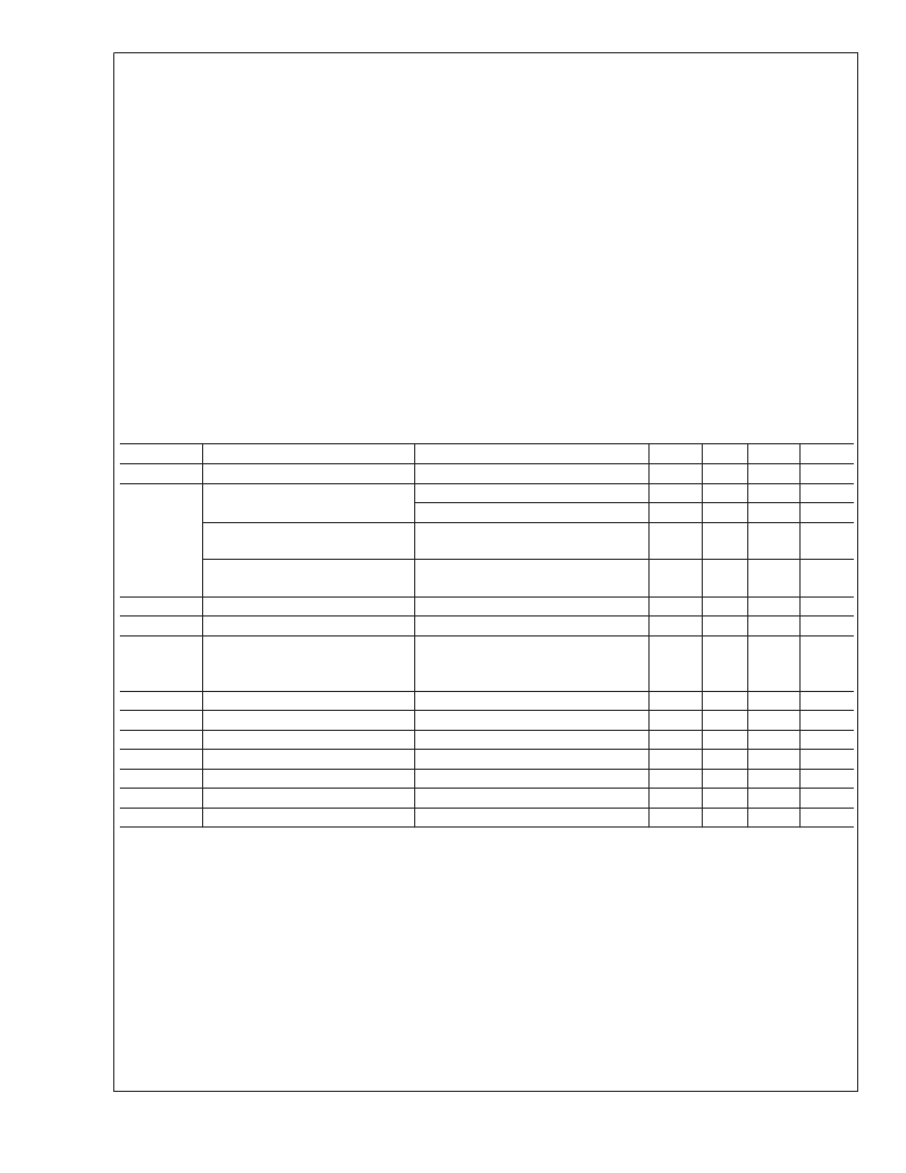
Absolute Maximum Ratings
(Note 1)
If Military/Aerospace specified devices are required,
please contact the National Semiconductor Sales Office/
Distributors for availability and specifications.
V
IN
Pin: Voltage to GND
FB, SW, EN Pin:
0.2V to 6.0V
(GND0.2V) to
(V
IN
+ 0.2V)
Internally Limited
Continuous Power Dissipation
(Note 3)
Junction Temperature (T
J-MAX
)
Storage Temperature Range
Maximum Lead Temperature
(Soldering, 10 sec.)
ESD Rating (Note 4)
Human Body Model:
V
IN
,GND,SW,FB
+125C
65C to +150C
260C
2.0 kV
Human Body Model: EN
Machine Model: All Pins
500V
200V
Operating Ratings
(Notes 1, 2)
Input Voltage Range
Recommended Load Current
Junction Temperature (T
J
) Range
Ambient Temperature (T
A
) Range (Note 5)
2.8V to 5.5V
0mA to 600 mA
25C to +125C
25C to +85C
Thermal Properties
Junction-to-Ambient
Thermal Resistance (
θ
JA
)
(SOT23-5) (Note 6)
250C/W
Electrical Characteristics
(Notes 2, 9, 10)
type apply over the full operating junction temperature range (25C
≤
T
J
≤
+125C). Unless otherwise noted, specifications
apply to the LM3671 Typical Application Circuit (Figure. 1) with V
IN
= EN = 3.6V, V
OUT
= 1.5V
Limits in standard typeface are for T
J
= 25C. Limits in
boldface
Symbol
V
IN
V
OUT
Parameter
Condition
Min
2.8
2
4
Typ
Max
5.5
+4
+4
Units
V
%
%
%/V
Input Voltage Range
Output Voltage
(Note 11)
I
O
= 0 mA
I
O
= 100 mA
2.8V
≤
V
IN
≤
5.5V
I
O
= 10 mA
100 mA
≤
I
O
≤
300 mA
V
IN
= 3.6V
(Note 7)
EN = 0V
No load, device is not switching (FB
forced higher than programmed output
voltage)
V
IN
= V
GS
= 3.6V
V
IN
= V
GS
= 3.6V
Open Loop (Note 8)
Line Regulation
0.045
Load Regulation
0.0031
%/mA
V
REF
I
SHDN
I
Q_PFM
Internal Reference Voltage
Shutdown Supply Current
DC Bias Current into V
IN
0.5
0.01
16
V
μA
μA
1
35
R
DSON (P)
R
DSON (N)
I
LIM
V
IH
V
IL
I
EN
F
OSC
Pin-Pin Resistance for PFET
Pin-Pin Resistance for NFET
Switch Peak Current Limit
Logic High Input
Logic Low Input
Enable (EN) Input Current
Internal Oscillator Frequency
380
250
1020
500
400
1150
m
m
mA
V
V
μA
MHz
830
1.0
0.4
1
2.6
0.01
2
PWM Mode
1.6
Note 1:
Absolute Maximum Ratings indicate limits beyond which damage to the component may occur. Operating Ratings are conditions under which operation of
the device is guaranteed. Operating Ratings do not imply guaranteed performance limits. For guaranteed performance limits and associated test conditions, see the
Electrical Characteristics tables.
Note 2:
All voltages are with respect to the potential at the GND pin.
Note 3:
Internal thermal shutdown circuitry protects the device from permanent damage. Thermal shutdown engages at T
J
= 150C (typ.) and disengages at T
J
=
130C (typ.).
Note 4:
The Human body model is a 100 pF capacitor discharged through a 1.5 k
resistor into each pin. The machine model is a 200 pF capacitor discharged
directly into each pin. MIL-STD-883 3015.7
Note 5:
In Applications where high power dissipation and/or poor package resistance is present, the maximum ambient temperature may have to be derated.
Maximum ambient temperature (T
) is dependent on the maximum operating junction temperature (T
), the maximum power dissipation of the device in
the application (P
) and the junction to ambient thermal resistance of the package (
θ
) in the application, as given by the following equation:T
A-MAX
= T
J-MAX
(
θ
JA
x P
D-MAX
). Refer to Dissipation rating table for P
D-MAX
values at different ambient temperatures.
Note 6:
Junction to ambient thermal resistance is highly application and board layout dependent. In applications where high power dissipation exists, special care
must be given to thermal dissipation issues in board design. Value specified here 250 C/W is based on measurement results using a 2 layer, 4" x 3", 2 oz Cu board
as per JEDEC standards. The (
θ
JA
) can be as low as 140 C/W if a 4 layer, 4" x 3", 2/1/1/2 oz. Cu board as per JEDEC standards is used.
Note 7:
For the ADJ version the resistor dividers should be selected such that at the desired output voltage,the voltage at the FB pin is 0.5V.
L
www.national.com
4
相關(guān)PDF資料 |
PDF描述 |
|---|---|
| LM3671MF-ADJ | 2MHz , 600mA Step-Down DC-DC Converter in SOT23-5 |
| LM3671MFX-1.2 | 2MHz , 600mA Step-Down DC-DC Converter in SOT23-5 |
| LM3671MFX-1.25 | 2MHz , 600mA Step-Down DC-DC Converter in SOT23-5 |
| LM3671MFX-1.375 | 2MHz , 600mA Step-Down DC-DC Converter in SOT23-5 |
| LM3671MFX-1.5 | 2MHz , 600mA Step-Down DC-DC Converter in SOT23-5 |
相關(guān)代理商/技術(shù)參數(shù) |
參數(shù)描述 |
|---|---|
| LM3671MF-2.5 | 功能描述:DC/DC 開(kāi)關(guān)控制器 RoHS:否 制造商:Texas Instruments 輸入電壓:6 V to 100 V 開(kāi)關(guān)頻率: 輸出電壓:1.215 V to 80 V 輸出電流:3.5 A 輸出端數(shù)量:1 最大工作溫度:+ 125 C 安裝風(fēng)格: 封裝 / 箱體:CPAK |
| LM3671MF-2.5/NOPB | 功能描述:DC/DC 開(kāi)關(guān)控制器 RoHS:否 制造商:Texas Instruments 輸入電壓:6 V to 100 V 開(kāi)關(guān)頻率: 輸出電壓:1.215 V to 80 V 輸出電流:3.5 A 輸出端數(shù)量:1 最大工作溫度:+ 125 C 安裝風(fēng)格: 封裝 / 箱體:CPAK |
| LM3671MF-2.8 | 功能描述:DC/DC 開(kāi)關(guān)控制器 RoHS:否 制造商:Texas Instruments 輸入電壓:6 V to 100 V 開(kāi)關(guān)頻率: 輸出電壓:1.215 V to 80 V 輸出電流:3.5 A 輸出端數(shù)量:1 最大工作溫度:+ 125 C 安裝風(fēng)格: 封裝 / 箱體:CPAK |
| LM3671MF-2.8/NOPB | 功能描述:DC/DC 開(kāi)關(guān)控制器 RoHS:否 制造商:Texas Instruments 輸入電壓:6 V to 100 V 開(kāi)關(guān)頻率: 輸出電壓:1.215 V to 80 V 輸出電流:3.5 A 輸出端數(shù)量:1 最大工作溫度:+ 125 C 安裝風(fēng)格: 封裝 / 箱體:CPAK |
| LM3671MF-3.3 | 功能描述:DC/DC 開(kāi)關(guān)控制器 RoHS:否 制造商:Texas Instruments 輸入電壓:6 V to 100 V 開(kāi)關(guān)頻率: 輸出電壓:1.215 V to 80 V 輸出電流:3.5 A 輸出端數(shù)量:1 最大工作溫度:+ 125 C 安裝風(fēng)格: 封裝 / 箱體:CPAK |
發(fā)布緊急采購(gòu),3分鐘左右您將得到回復(fù)。