- 您現(xiàn)在的位置:買賣IC網(wǎng) > PDF目錄367565 > LM4766TF AUDIO AMPLIFIER|DUAL|BIPOLAR|ZIP|15PIN|PLASTIC PDF資料下載
參數(shù)資料
| 型號: | LM4766TF |
| 元件分類: | 音頻放大器 |
| 英文描述: | AUDIO AMPLIFIER|DUAL|BIPOLAR|ZIP|15PIN|PLASTIC |
| 中文描述: | 音頻放大器|雙|雙極|郵政編碼| 15針|塑料 |
| 文件頁數(shù): | 7/15頁 |
| 文件大?。?/td> | 480K |
| 代理商: | LM4766TF |

External Components Description
Components
R
B
Functional Description
1
Prevents currents from entering the amplifier’s non-inverting input which may be passed through to the
load upon power down of the system due to the low input impedance of the circuitry when the
undervoltage circuitry is off. This phenomenon occurs when the supply voltages are below 1.5V.
Inverting input resistance to provide AC gain in conjunction with R
f
.
Feedback resistance to provide AC gain in conjunction with R
i
.
Feedback capacitor which ensures unity gain at DC. Also creates a highpass filter with R
i
at f
C
=
1/(2
π
R
i
C
i
).
Provides power supply filtering and bypassing. Refer to the Supply Bypassing application section for
proper placement and selection of bypass capacitors.
Acts as a volume control by setting the input voltage level.
2
3
4
R
i
R
f
C
i
(Note 14)
C
S
5
6
R
V
(Note 14)
R
IN
(Note 14)
C
IN
(Note 14)
R
SN
(Note 14)
C
SN
(Note 14)
L (Note 14)
7
Sets the amplifier’s input terminals DC bias point when C
IN
is present in the circuit. Also works with C
IN
to
create a highpass filter at f
C
= 1/(2
π
R
IN
C
IN
). Refer to Figure 4
Input capacitor which blocks the input signal’s DC offsets from being passed onto the amplifier’s inputs.
8
9
Works with C
SN
to stabilize the output stage by creating a pole that reduces high frequency instabilities.
10
Works with R
SN
to stabilize the output stage by creating a pole that reduces high frequency instabilities.
The pole is set at f
C
= 1/(2
π
R
SN
C
SN
). Refer to Figure 4
Provides high impedance at high frequencies so that R may decouple a highly capacitive load and reduce
the Q of the series resonant circuit. Also provides a low impedance at low frequencies to short out R and
pass audio signals to the load. Refer to Figure 4
Provides DC voltage biasing for the transistor Q1 in single supply operation.
Provides bias filtering for single supply operation.
Limits the voltage difference between the amplifier’s inputs for single supply operation. Refer to the
Clicks
and Pops
application section for a more detailed explanation of the function of R
INP
.
Provides input bias current for single supply operation. Refer to the
Clicks and Pops
application section
for a more detailed explanation of the function of R
BI
.
Establishes a fixed DC current for the transistor Q1 in single supply operation. This resistor stabilizes the
half-supply point along with C
A
.
Mute resistance set up to allow 0.5mA to be drawn from pin 6 or 11 to turn the muting function off.
→
R
M
is calculated using: R
M
≤
(|V
EE
| 2.6V)/l where l
≥
0.5mA. Refer to the Mute Attenuation vs Mute
Current curves in the Typical Performance Characteristics section.
Mute capacitance set up to create a large time constant for turn-on and turn-off muting.
Mute switch that mutes the music going into the amplifier when opened.
11
12
R (Note 14)
13
14
15
R
A
C
A
R
INP
(Note 14)
R
BI
16
17
R
E
18
R
M
19
20
C
M
S
1
Note 14:
Optional components dependent upon specific design requirements.
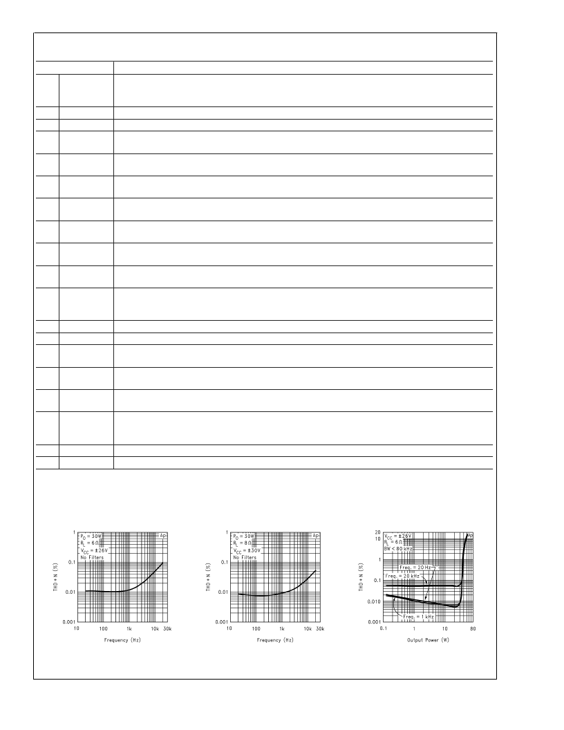
Typical Performance Characteristics
THD+N vs Frequency
DS100928-55
THD+N vs Frequency
DS100928-56
THD+N vs Output Power
DS100928-58
L
www.national.com
7
相關(guān)PDF資料 |
PDF描述 |
|---|---|
| LM4836MTEX | Dual Audio Amplifier |
| LM4836MTX | Dual Audio Amplifier |
| LM4851IBL-1 | Amplifier. Other |
| LM4854LD | AUDIO AMPLIFIER|DUAL|LLCC|14PIN|CERAMIC |
| LM4854MM | AUDIO AMPLIFIER|DUAL|TSSOP|10PIN|PLASTIC |
相關(guān)代理商/技術(shù)參數(shù) |
參數(shù)描述 |
|---|---|
| LM4766TF/NOPB | 功能描述:音頻放大器 RoHS:否 制造商:STMicroelectronics 產(chǎn)品:General Purpose Audio Amplifiers 輸出類型:Digital 輸出功率: THD + 噪聲: 工作電源電壓:3.3 V 電源電流: 最大功率耗散: 最大工作溫度: 安裝風(fēng)格:SMD/SMT 封裝 / 箱體:TQFP-64 封裝:Reel |
| LM4766TF/NOPB | 制造商:Texas Instruments 功能描述:Audio Power Amplifier IC |
| LM476-S | 功能描述:基本/快動(dòng)開關(guān) Foot Switch RoHS:否 制造商:Omron Electronics 觸點(diǎn)形式:SPDT 執(zhí)行器:Lever 電流額定值:5 A 電壓額定值 AC:250 V 電壓額定值 DC:30 V 功率額定值: 工作力:120 g IP 等級:IP 67 NEMA 額定值: 端接類型:Wire 安裝:Panel |
| LM4780 | 制造商:NSC 制造商全稱:National Semiconductor 功能描述:Audio Power Amplifier Series Stereo 60W, Mono 120W Audio Power Amplifier with Mute |
| LM4780TA | 功能描述:音頻放大器 RoHS:否 制造商:STMicroelectronics 產(chǎn)品:General Purpose Audio Amplifiers 輸出類型:Digital 輸出功率: THD + 噪聲: 工作電源電壓:3.3 V 電源電流: 最大功率耗散: 最大工作溫度: 安裝風(fēng)格:SMD/SMT 封裝 / 箱體:TQFP-64 封裝:Reel |
發(fā)布緊急采購,3分鐘左右您將得到回復(fù)。