- 您現(xiàn)在的位置:買賣IC網(wǎng) > PDF目錄8610 > LTC6400IUD-14#PBF (Linear Technology)IC ADC DRIVER DIFF 2.4GHZ 16QFN PDF資料下載
參數(shù)資料
| 型號(hào): | LTC6400IUD-14#PBF |
| 廠商: | Linear Technology |
| 文件頁數(shù): | 3/16頁 |
| 文件大小: | 0K |
| 描述: | IC ADC DRIVER DIFF 2.4GHZ 16QFN |
| 標(biāo)準(zhǔn)包裝: | 121 |
| 類型: | ADC 驅(qū)動(dòng)器 |
| 應(yīng)用: | 數(shù)據(jù)采集 |
| 安裝類型: | 表面貼裝 |
| 封裝/外殼: | 16-WFQFN 裸露焊盤 |
| 供應(yīng)商設(shè)備封裝: | 16-QFN-EP(3x3) |
| 包裝: | 管件 |

LTC6400-14
11
640014fb
APPLICATIONS INFORMATION
Circuit Operation
The LTC6400-14 is a low noise and low distortion fully
differential op amp/ADC driver with:
Operation from DC to 2.4GHz (–3dB bandwidth)
Fixed gain of 5V/V (14dB)
Differential input impedance 200
Ω
Differential output impedance 25
Ω
On-Chip 590MHz output lter
The LTC6400 is composed of a fully differential amplier
with on chip feedback and output common mode voltage
control circuitry. Differential gain and input impedance are
set by 100
Ω/1000Ω resistors in the feedback network.
Small output resistors of 12.5
Ωimprovethecircuitstability
over various load conditions. They also provide a possible
external ltering option, which is often desirable when the
load is an ADC.
Filter resistors of 50
Ω are available for additional ltering.
Lowpass/bandpass lters are easily implemented with
just a couple of external components. Moreover, they of-
fer single-ended 50
Ω matching in wideband applications
and no external resistor is needed.
The LTC6400-14 is very exible in terms of I/O coupling.
It can be AC- or DC-coupled at the inputs, the outputs or
both. Due to the internal connection between input and
output, users are advised to keep input common mode
voltage between 1V and 1.8V for proper operation. If the
inputs are AC-coupled, the input common mode voltage
is automatically biased approximately 450mV above VOCM
and thus no external circuitry is needed for bias. The
LTC6400-14 provides an output common mode voltage
set by VOCM, which allows driving an ADC directly without
external components such as a transformer or AC coupling
capacitors. The input signal can be either single-ended
or differential with only minor differences in distortion
performance.
Input Impedance and Matching
The differential input impedance of the LTC6400-14 is
200
Ω. If a 200Ω source impedance is unavailable, then
the differential inputs may need to be terminated to a lower
value impedance, e.g. 50
Ω, in order to provide an imped-
ance match for the source. Several choices are available.
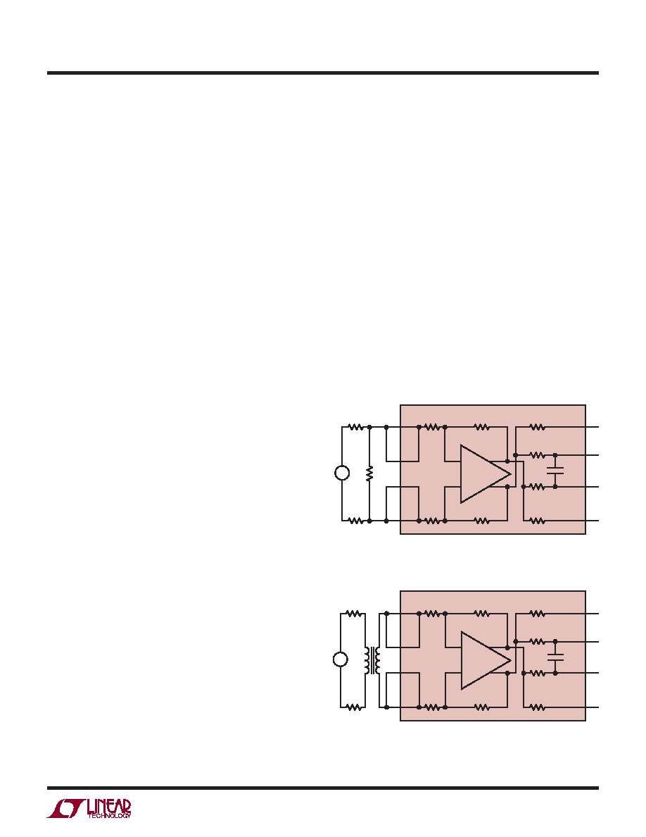
One approach is to use a differential shunt resistor (Figure
1). Another approach is to employ a wide band transformer
(Figure 2). Both methods provide a wide band impedance
match. The termination resistor or the transformer must
be placed close to the input pins in order to minimize
the reection due to input mismatch. Alternatively, one
could apply a narrowband impedance match at the inputs
of the LTC6400-14 for frequency selection and/or noise
reduction.
Referring to Figure 3, LTC6400-14 can be easily congured
for single-ended input and differential output without a
balun. The signal is fed to one of the inputs through a
matching network while the other input is connected to the
same matching network and a source resistor. Because the
return ratios of the two feedback paths are equal, the two
outputs have the same gain and thus symmetrical swing.
Figure 1. Input Termination for Differential 50
Ω Input Impedance
Using Shunt Resistor
Figure 2. Input Termination for Differential 50
Ω Input Impedance
Using a 1:4 Balun
640014 F01
+OUT
+OUTF
–OUTF
–OUT
+IN
IN+
OUT–
IN–
OUT+
+IN
–IN
100Ω
66.5Ω
12.5Ω
500Ω
LTC6400-14
100Ω
25Ω
VIN
500Ω
12.5Ω
50Ω
2.7pF
13
14
15
16
7
5
6
8
+
–
640014 F02
+OUT
+OUTF
–OUTF
–OUT
+IN
IN+
OUT–
IN–
OUT+
+IN
–IN
100Ω
12.5Ω
500Ω
LTC6400-14
100Ω
25Ω
VIN
500Ω
12.5Ω
50Ω
2.7pF
13
14
15
16
7
5
6
8
+
–
1:4
MINI-CIRCUITS
TCM4-19
相關(guān)PDF資料 |
PDF描述 |
|---|---|
| VE-243-IV-F4 | CONVERTER MOD DC/DC 24V 150W |
| SY88843VEY TR | IC AMP POST PECL 3.3V/5V 10MSOP |
| VE-B4D-MV-B1 | CONVERTER MOD DC/DC 85V 150W |
| AD7398BR-REEL | IC DAC 12BIT QUAD SRL 16-SOIC |
| SY88923AVKG TR | IC POST AMP HS LIMITING 10-MSOP |
相關(guān)代理商/技術(shù)參數(shù) |
參數(shù)描述 |
|---|---|
| LTC6400IUD-14-TRPBF | 制造商:LINER 制造商全稱:Linear Technology 功能描述:2.4GHz Low Noise, Low Distortion Differential ADC Driver for 300MHz IF |
| LTC6400IUD-20#PBF | 功能描述:IC ADC DRIVER DIFF 16-QFN RoHS:是 類別:集成電路 (IC) >> 線性 - 放大器 - 專用 系列:- 產(chǎn)品培訓(xùn)模塊:Lead (SnPb) Finish for COTS Obsolescence Mitigation Program 標(biāo)準(zhǔn)包裝:60 系列:- 類型:可變?cè)鲆娣糯笃?應(yīng)用:CATV 安裝類型:表面貼裝 封裝/外殼:20-WQFN 裸露焊盤 供應(yīng)商設(shè)備封裝:20-TQFN-EP(5x5) 包裝:托盤 |
| LTC6400IUD-20#TRPBF | 功能描述:IC ADC DRIVER DIFF 16-QFN RoHS:是 類別:集成電路 (IC) >> 線性 - 放大器 - 專用 系列:- 產(chǎn)品培訓(xùn)模塊:Lead (SnPb) Finish for COTS Obsolescence Mitigation Program 標(biāo)準(zhǔn)包裝:60 系列:- 類型:可變?cè)鲆娣糯笃?應(yīng)用:CATV 安裝類型:表面貼裝 封裝/外殼:20-WQFN 裸露焊盤 供應(yīng)商設(shè)備封裝:20-TQFN-EP(5x5) 包裝:托盤 |
| LTC6400IUD-20-PBF | 制造商:LINER 制造商全稱:Linear Technology 功能描述:1.8GHz Low Noise, Low Distortion Differential ADC Driver for 300MHz IF |
| LTC6400IUD-20-TRPBF | 制造商:LINER 制造商全稱:Linear Technology 功能描述:1.8GHz Low Noise, Low Distortion Differential ADC Driver for 300MHz IF |
發(fā)布緊急采購(gòu),3分鐘左右您將得到回復(fù)。