- 您現(xiàn)在的位置:買賣IC網(wǎng) > PDF目錄8610 > LTC6400IUD-14#PBF (Linear Technology)IC ADC DRIVER DIFF 2.4GHZ 16QFN PDF資料下載
參數(shù)資料
| 型號(hào): | LTC6400IUD-14#PBF |
| 廠商: | Linear Technology |
| 文件頁數(shù): | 5/16頁 |
| 文件大小: | 0K |
| 描述: | IC ADC DRIVER DIFF 2.4GHZ 16QFN |
| 標(biāo)準(zhǔn)包裝: | 121 |
| 類型: | ADC 驅(qū)動(dòng)器 |
| 應(yīng)用: | 數(shù)據(jù)采集 |
| 安裝類型: | 表面貼裝 |
| 封裝/外殼: | 16-WFQFN 裸露焊盤 |
| 供應(yīng)商設(shè)備封裝: | 16-QFN-EP(3x3) |
| 包裝: | 管件 |

LTC6400-14
13
640014fb
which is dominated by a low pass lter connected to the
VOCM pin and is aimed to reduce common mode noise
generation at the outputs. The internal common mode
feedback loop has a –3dB bandwidth around 400MHz,
allowing fast common mode rejection at the outputs of
the LTC6400-14. The VOCM pin should be tied to a DC bias
voltage with a 0.1μF bypass capacitor. When interfacing
with A/D converters such as the LTC22xx families, the VOCM
pin can be connected to the VCM pin of the ADC.
Driving A/D Converters
The LTC6400-14 has been specically designed to inter-
face directly with high speed A/D converters. In Figure 7,
an example schematic shows the LTC6400-14 with a
single-ended input driving the LTC2208, which is a 16-bit,
130Msps ADC. Two external 4.99
Ωresistorshelpeliminate
potential resonance associated with stray capacitance of
PCB traces and bond wires of either the ADC input or the
driver output. VOCM of the LTC6400-14 is connected to VCM
of the LTC2208 VCM pin at 1.25V. Alternatively, a single-
ended input signal can be converted to a differential signal
via a balun and fed to the input of the LTC6400-14.
Figure 8 summarizes the IMD3 of the whole system in
Figure 7. Note that Figure 7 shows a direct connection
to the LTC2208, but in many applications an anti-alias
lter would be desirable to limit the wideband noise of
the amplier. This is especially true in high performance
16-bit designs.
Test Circuits
Due to the fully-differential design of the LTC6400 and
its usefulness in applications with differing characteristic
Figure 7. Single-Ended Input to LTC6400-14 and LTC2208
Figure 8. IMD3 for the Combination of LTC6400-14 and LTC2208
APPLICATIONS INFORMATION
29Ω
66.5Ω
0.1μF
640014 F07
LTC6400-14
VOCM
ENABLE
IF IN
LTC2208
4.99Ω
0.1μF
LTC2208 130Msps
16-Bit ADC
1.25V
4.99Ω
14dB GAIN
AIN–
AIN+
VCM
–IN
+IN
+OUT
+OUTF
–OUTF
–OUT
FREQUENCY (MHz)
0
IMD3
(dBc)
–40
–110
–100
–90
–80
–70
–60
–50
100
150
50
200
640014 F08
250
300
SINGLE-ENDED INPUT
fS = 122.8Msps
DRIVER VOUT = 2VP-P COMPOSITE
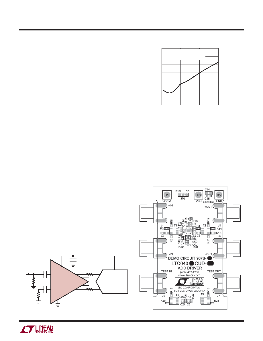
Top Silkscreen
specications, two test circuits are used to generate the
information in this datasheet. Test Circuit A is DC987B,
a two-port demonstration circuit for the LTC6400 family.
The schematic and silkscreen are shown below. This
circuit includes input and output transformers (baluns)
for single-ended-to-differential conversion and impedance
transformation, allowing direct hook-up to a 2-port
相關(guān)PDF資料 |
PDF描述 |
|---|---|
| VE-243-IV-F4 | CONVERTER MOD DC/DC 24V 150W |
| SY88843VEY TR | IC AMP POST PECL 3.3V/5V 10MSOP |
| VE-B4D-MV-B1 | CONVERTER MOD DC/DC 85V 150W |
| AD7398BR-REEL | IC DAC 12BIT QUAD SRL 16-SOIC |
| SY88923AVKG TR | IC POST AMP HS LIMITING 10-MSOP |
相關(guān)代理商/技術(shù)參數(shù) |
參數(shù)描述 |
|---|---|
| LTC6400IUD-14-TRPBF | 制造商:LINER 制造商全稱:Linear Technology 功能描述:2.4GHz Low Noise, Low Distortion Differential ADC Driver for 300MHz IF |
| LTC6400IUD-20#PBF | 功能描述:IC ADC DRIVER DIFF 16-QFN RoHS:是 類別:集成電路 (IC) >> 線性 - 放大器 - 專用 系列:- 產(chǎn)品培訓(xùn)模塊:Lead (SnPb) Finish for COTS Obsolescence Mitigation Program 標(biāo)準(zhǔn)包裝:60 系列:- 類型:可變?cè)鲆娣糯笃?應(yīng)用:CATV 安裝類型:表面貼裝 封裝/外殼:20-WQFN 裸露焊盤 供應(yīng)商設(shè)備封裝:20-TQFN-EP(5x5) 包裝:托盤 |
| LTC6400IUD-20#TRPBF | 功能描述:IC ADC DRIVER DIFF 16-QFN RoHS:是 類別:集成電路 (IC) >> 線性 - 放大器 - 專用 系列:- 產(chǎn)品培訓(xùn)模塊:Lead (SnPb) Finish for COTS Obsolescence Mitigation Program 標(biāo)準(zhǔn)包裝:60 系列:- 類型:可變?cè)鲆娣糯笃?應(yīng)用:CATV 安裝類型:表面貼裝 封裝/外殼:20-WQFN 裸露焊盤 供應(yīng)商設(shè)備封裝:20-TQFN-EP(5x5) 包裝:托盤 |
| LTC6400IUD-20-PBF | 制造商:LINER 制造商全稱:Linear Technology 功能描述:1.8GHz Low Noise, Low Distortion Differential ADC Driver for 300MHz IF |
| LTC6400IUD-20-TRPBF | 制造商:LINER 制造商全稱:Linear Technology 功能描述:1.8GHz Low Noise, Low Distortion Differential ADC Driver for 300MHz IF |
發(fā)布緊急采購(gòu),3分鐘左右您將得到回復(fù)。