- 您現(xiàn)在的位置:買賣IC網(wǎng) > PDF目錄44998 > LTC6604CUFF-15#TRPBF (LINEAR TECHNOLOGY CORP) SPECIALTY ANALOG CIRCUIT, PQCC34 PDF資料下載
參數(shù)資料
| 型號: | LTC6604CUFF-15#TRPBF |
| 廠商: | LINEAR TECHNOLOGY CORP |
| 元件分類: | 模擬信號調(diào)理 |
| 英文描述: | SPECIALTY ANALOG CIRCUIT, PQCC34 |
| 封裝: | 4 X 7 MM, 0.75 MM HEIGHT, LEAD FREE, PLASTIC, QFN-34 |
| 文件頁數(shù): | 3/16頁 |
| 文件大小: | 203K |
| 代理商: | LTC6604CUFF-15#TRPBF |
LT6604-15
11
660415fa
APPLICATIONS INFORMATION
where impedance must be considered is the evaluation of
the LT6604-15 with a network analyzer.
Figure 5 is a laboratory setup that can be used to char-
acterize the LT6604-15 using single-ended instruments
with 50Ω source impedance and 50Ω input impedance.
For a unity gain conguration the LT6604-15 requires
an 536Ω source resistance yet the network analyzer
output is calibrated for a 50Ω load resistance. The 1:1
transformer, 52.3Ω and 523Ω resistors satisfy the two
constraints above. The transformer converts the single-
ended source into a differential stimulus. Similarly, the
output of the LT6604-15 will have lower distortion with
larger load resistance yet the analyzer input is typically
50Ω. The 4:1 turns (16:1 impedance) transformer and the
two 402Ω resistors of Figure 5, present the output of the
LT6604-15 with a 1600Ω differential load, or the equiva-
lent of 800Ω to ground at each output. The impedance
seen by the network analyzer input is still 50Ω, reducing
reections in the cabling between the transformer and
analyzer input.
Differential and Common Mode Voltage Ranges
The differential ampliers inside the LT6604-15 contain
circuitry to limit the maximum peak-to-peak differential
voltage through the lter. This limiting function prevents
excessive power dissipation in the internal circuitry and
provides output short-circuit protection. The limiting
function begins to take effect at output signal levels
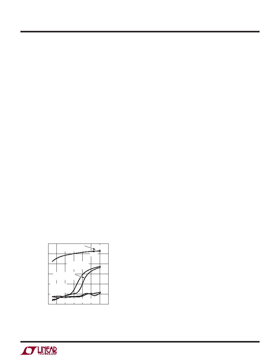
above 2VP-P and it becomes noticeable above 3.5VP-P.
This is illustrated in Figure 6; the LT6604-15 channel was
congured with unity passband gain and the input of the
lter was driven with a 1MHz signal. Because this voltage
limiting takes place well before the output stage of the
lter reaches the supply rails, the input/output behavior
of the IC shown in Figure 6 is relatively independent of
the power supply voltage.
The two ampliers inside the LT6604-15 channel have
independent control of their output common mode voltage
(see the Block Diagram section). The following guidelines
will optimize the performance of the lter.
VMID can be allowed to oat, but it must be bypassed to an
AC ground with a 0.01μF capacitor or some instability may
be observed. VMID can be driven from a low impedance
source, provided it remains at least 1.5V above V– and at
least 1.5V below V+. An internal resistor divider sets the
voltage of VMID. While the internal 11k resistors are well
matched, their absolute value can vary by ±20%. This
should be taken into consideration when connecting an
external resistor network to alter the voltage of VMID.
VOCM can be shorted to VMID for simplicity. If a different
common mode output voltage is required, connect VOCM
to a voltage source or resistor network. For 3V and 3.3V
supplies the voltage at VOCM must be less than or equal
to the mid supply level. For example, voltage (VOCM) ≤
1.65V on a single 3.3V supply. For power supply voltages
higher than 3.3V the voltage at VOCM can be set above mid
supply. The voltage on VOCM should not be more than 1V
below the voltage on VMID. The voltage on VOCM should
not be more than 2V above the voltage on VMID. VOCM is
a high impedance input.
The LT6604-15 was designed to process a variety of input
signals including signals centered on the mid-supply volt-
age and signals that swing between ground and a positive
voltage in a single supply system (Figure 1). The range of
allowable input common mode voltage (the average of VIN+
and VIN– in Figure 1) is determined by the power supply
level and gain setting (see Distortion vs Input Common
Mode Level in the Typical Performance Characteristics).
1MHz INPUT LEVEL (VP-P)
0
20
0
–20
–40
–60
–80
–100
35
660415 F06
12
46
7
OUTPUT
LEVEL
(dBV)
3RD HARMONIC
85°C
1dB COMPRESSION
POINTS
25°C
85°C
3RD HARMONIC
25°C
2ND HARMONIC, 25°C
2ND
HARMONIC
85°C
Figure 6. Output Level vs Input Level, Differential
1MHz Input, Gain = 1
相關(guān)PDF資料 |
PDF描述 |
|---|---|
| LTC6652AHMS8-2.5 | 1-OUTPUT THREE TERM VOLTAGE REFERENCE, 2.5 V, PDSO8 |
| LTC6652BHMS8-2.5 | 1-OUTPUT THREE TERM VOLTAGE REFERENCE, 2.5 V, PDSO8 |
| LTC6801HG#TRPBF | 1-CHANNEL POWER SUPPLY SUPPORT CKT, PDSO36 |
| LTC6801IG#TRPBF | 1-CHANNEL POWER SUPPLY SUPPORT CKT, PDSO36 |
| LTC6801IG#PBF | 1-CHANNEL POWER SUPPLY SUPPORT CKT, PDSO36 |
相關(guān)代理商/技術(shù)參數(shù) |
參數(shù)描述 |
|---|---|
| LTC6604IUFF-10-TRPBF | 制造商:LINER 制造商全稱:Linear Technology 功能描述:Dual Very Low Noise, Differential Amplifi er and 10MHz Lowpass Filter |
| LTC6604IUFF-15-TRPBF | 制造商:LINER 制造商全稱:Linear Technology 功能描述:Dual Very Low Noise, Differential Amplifi er and 15MHz Lowpass Filter |
| LTC6605-10 | 制造商:LINER 制造商全稱:Linear Technology 功能描述:16-Bit, 20Msps Low Power ADC |
| LTC6605-14 | 制造商:LINER 制造商全稱:Linear Technology 功能描述:16-Bit, 20Msps Low Power ADC |
| LTC6605-7 | 制造商:LINER 制造商全稱:Linear Technology 功能描述:16-Bit, 20Msps Low Power Dual ADC |
發(fā)布緊急采購,3分鐘左右您將得到回復(fù)。