- 您現(xiàn)在的位置:買(mǎi)賣(mài)IC網(wǎng) > PDF目錄44998 > LTC6604CUFF-15#TRPBF (LINEAR TECHNOLOGY CORP) SPECIALTY ANALOG CIRCUIT, PQCC34 PDF資料下載
參數(shù)資料
| 型號(hào): | LTC6604CUFF-15#TRPBF |
| 廠商: | LINEAR TECHNOLOGY CORP |
| 元件分類(lèi): | 模擬信號(hào)調(diào)理 |
| 英文描述: | SPECIALTY ANALOG CIRCUIT, PQCC34 |
| 封裝: | 4 X 7 MM, 0.75 MM HEIGHT, LEAD FREE, PLASTIC, QFN-34 |
| 文件頁(yè)數(shù): | 5/16頁(yè) |
| 文件大小: | 203K |
| 代理商: | LTC6604CUFF-15#TRPBF |
第1頁(yè)第2頁(yè)第3頁(yè)第4頁(yè)當(dāng)前第5頁(yè)第6頁(yè)第7頁(yè)第8頁(yè)第9頁(yè)第10頁(yè)第11頁(yè)第12頁(yè)第13頁(yè)第14頁(yè)第15頁(yè)第16頁(yè)
LT6604-15
13
660415fa
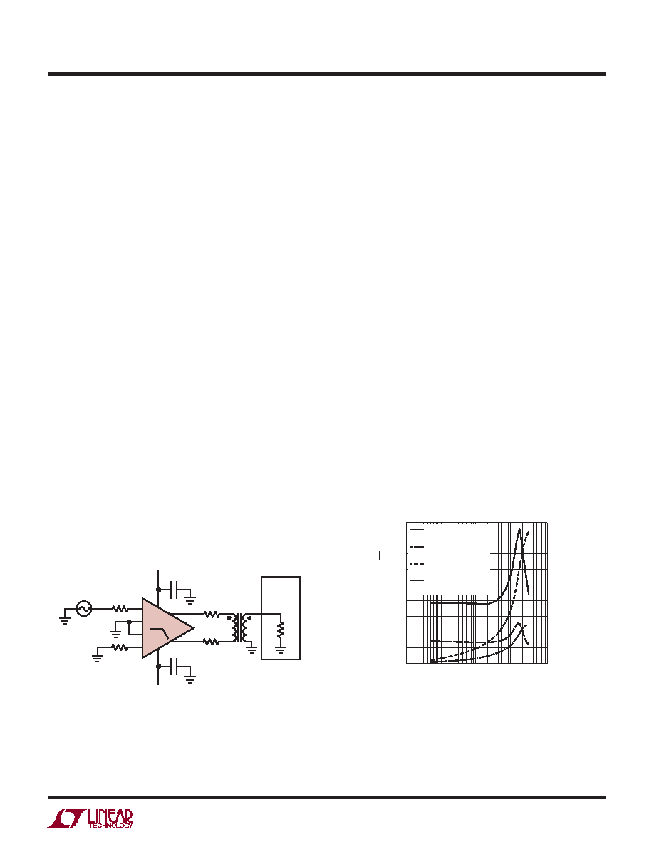
Figure 8 is plot of the noise spectral density as a function
of frequency for an LT6604-15 with RIN = 536Ω using
the xture of Figure 7 (the instrument noise has been
subtracted from the results). The noise at each output
is comprised of a differential component and a common
mode component. Using a transformer or combiner to
convert the differential outputs to single-ended signal
rejects the common mode noise and gives a true measure
of the S/N achievable in the system. Conversely, if each
output is measured individually and the noise power added
together, the resulting calculated noise level will be higher
than the true differential noise.
Power Dissipation
The LT6604-15 ampliers combine high speed with large
signal currents in a small package. There is a need to en-
sure that the die’s junction temperature does not exceed
150°C. The LT6604-15 has an Exposed Pad (pin 35) which
is connected to the lower supply (V–). Connecting the pad
to a ground plane helps to dissipate the heat generated
by the chip. Metal trace and plated through-holes can be
used to spread the heat generated by the device to the
backside of the PC board.
Junction temperature, TJ, is calculated from the ambient
temperature, TA, and power dissipation, PD. The power
dissipation is the product of supply voltage, VS, and
supply current, IS. Therefore, the junction temperature
is given by:
TJ = TA + (PD θJA) = TA + (VS IS θJA)
where the supply current, IS,isafunctionofsignallevel,load
impedance, temperature and common mode voltages. For
a given supply voltage, the worst-case power dissipation
occurs when the differential input signal is maximum, the
common mode currents are maximum (see Applications
Information regarding Common Mode DC Currents), the
load impedance is small and the ambient temperature is
maximum. To compute the junction temperature, measure
the supply current under these worstcase conditions, use
34°C/W as the package thermal resistance, then apply the
equation for TJ. For example, using the circuit in Figure 3
with DC differential input voltage of 250mV, a differential
output voltage of 1V, no load resistance and an ambient
temperature of 85°C, the supply current (current into V+)
measures 50mA The resulting junction temperature is:
TJ = TA + (PD θJA) = 85 + (5 2 0.05 34) = 102°C.
The thermal resistance can be affected by the amount of
copper on the PCB that is connected to V–. The thermal
resistance of the circuit can increase if the exposed pad
is not connected to a large ground plane with a number
of vias.
APPLICATIONS INFORMATION
–
+
0.1μF
2.5V
–2.5V
–
+
LT6604-15
25
27
4
34
6
2
29
7
RIN
25Ω
660415 F07
SPECTRUM
ANALYZER
INPUT
50Ω
VIN
COILCRAFT
TTWB-1010
1:1
1/2
FREQUENCY (MHz)
10
NOISE
DENSIT
Y
(nV
RMS
/√Hz)
INTEGRA
TED
NOISE
(μ
V)
20
25
35
45
40
0.01
1
10
100
660415 F08
0
0.1
30
15
5
40
80
100
140
180
160
0
120
60
20
NOISE DENSITY,
GAIN = 1x
NOISE DENSITY,
GAIN = 4x
INTEGRATED NOISE,
GAIN = 1x
INTEGRATED NOISE,
GAIN = 4x
Figure 7
Figure 8. Input Referred Noise, Gain = 1
相關(guān)PDF資料 |
PDF描述 |
|---|---|
| LTC6652AHMS8-2.5 | 1-OUTPUT THREE TERM VOLTAGE REFERENCE, 2.5 V, PDSO8 |
| LTC6652BHMS8-2.5 | 1-OUTPUT THREE TERM VOLTAGE REFERENCE, 2.5 V, PDSO8 |
| LTC6801HG#TRPBF | 1-CHANNEL POWER SUPPLY SUPPORT CKT, PDSO36 |
| LTC6801IG#TRPBF | 1-CHANNEL POWER SUPPLY SUPPORT CKT, PDSO36 |
| LTC6801IG#PBF | 1-CHANNEL POWER SUPPLY SUPPORT CKT, PDSO36 |
相關(guān)代理商/技術(shù)參數(shù) |
參數(shù)描述 |
|---|---|
| LTC6604IUFF-10-TRPBF | 制造商:LINER 制造商全稱(chēng):Linear Technology 功能描述:Dual Very Low Noise, Differential Amplifi er and 10MHz Lowpass Filter |
| LTC6604IUFF-15-TRPBF | 制造商:LINER 制造商全稱(chēng):Linear Technology 功能描述:Dual Very Low Noise, Differential Amplifi er and 15MHz Lowpass Filter |
| LTC6605-10 | 制造商:LINER 制造商全稱(chēng):Linear Technology 功能描述:16-Bit, 20Msps Low Power ADC |
| LTC6605-14 | 制造商:LINER 制造商全稱(chēng):Linear Technology 功能描述:16-Bit, 20Msps Low Power ADC |
| LTC6605-7 | 制造商:LINER 制造商全稱(chēng):Linear Technology 功能描述:16-Bit, 20Msps Low Power Dual ADC |
發(fā)布緊急采購(gòu),3分鐘左右您將得到回復(fù)。