- 您現(xiàn)在的位置:買賣IC網(wǎng) > PDF目錄367613 > LUCL8576BP-DT Dual Ringing SLIC PDF資料下載
參數(shù)資料
| 型號(hào): | LUCL8576BP-DT |
| 英文描述: | Dual Ringing SLIC |
| 中文描述: | 雙振鈴用戶接口 |
| 文件頁(yè)數(shù): | 23/26頁(yè) |
| 文件大小: | 583K |
| 代理商: | LUCL8576BP-DT |
第1頁(yè)第2頁(yè)第3頁(yè)第4頁(yè)第5頁(yè)第6頁(yè)第7頁(yè)第8頁(yè)第9頁(yè)第10頁(yè)第11頁(yè)第12頁(yè)第13頁(yè)第14頁(yè)第15頁(yè)第16頁(yè)第17頁(yè)第18頁(yè)第19頁(yè)第20頁(yè)第21頁(yè)第22頁(yè)當(dāng)前第23頁(yè)第24頁(yè)第25頁(yè)第26頁(yè)

Agere Systems Inc.
23
Data Sheet
May 2001
L8576B Dual Ringing SLIC
Applications
(continued)
ac Design
(continued)
Receive Gain
Ratios of R
RCV
, R
T1
, R
GP
will set both the low-frequency
termination and receive gain for the complex case. In
the complex case, additional high-frequency compen-
sation, via C
N
, R
N1
, and R
N2
, is needed for the return
loss characteristic. For resistive termination, C
N
, R
N1
,
and R
N2
are not used and R
CVN
is tied to ground and a
resistor.
Determine the receive gain, G
RCV
, taking into account
the impedance transformation in a manner similar to
transmit gain.
R
X
(dB) = R
X (specified[dB])
+ 20log
R
X
(dB) = 20log G
RCV
Then:
G
RCV
=
and low-frequency termination
Z
TER(low)
=
+ 2R
P
EQ
600
R
1
R
T1
---------------
R
GP
---------------
+
+
-----------------------------------------------
GP
1
-----------
RCV
---------------
+
+
--------------------------------------------
Z
TER(low)
is the specified termination impedance assum-
ing low frequency (C or C
′ is open).
R
P
is the series protection resistor.
These two equations are best solved using a computer
spreadsheet.
Next, solve for the high-frequency return loss compen-
sation circuit, C
N
, R
N1
, and R
N2
:
C
N
x
R
N2
=
C
TGS
x
R
TGP
R
N1
= R
N2
There is an input offset voltage associated with nodes
R
CVN
, R
CVP
. To minimize the effect of the mismatch of
this voltage at T/R, the equivalent resistance to ac
ground at R
CVN
should be approximately equal to that
at R
CVP
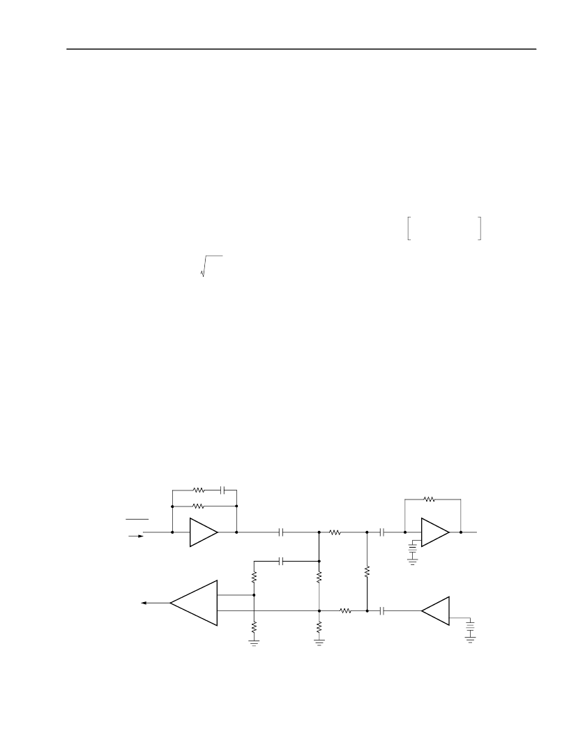
. Refer to Figure 22 (schematic with dc blocking
capacitors). To meet this requirement, R
N2
= R
GP
|| R
T1
.
Hybrid Balance
Set the hybrid cancellation via R
HB
.
R
HB
=
If a +5 V only codec such as an Agere T8503 is used,
dc blocking capacitors must be added as shown in
Figure 22. This is because the codec is referenced to
+2.5 V and the SLIC to ground. With the ac coupling, a
dc bias at T/R is eliminated and power associated with
this bias is not consumed.
P
1500
2R
1500
2R
P
------------R
R
TGP
-------------
1
–
RCV
TX
×
---------------------------------
5-8413 (F)
Figure 22. ac Interface Circuit Using First-Generation Codec (Including Blocking Capacitors)
R
TGS
R
TSP
= 24.4 k
V
ITR
R
X
R
HB
CODEC OUTPUT
DRIVE AMP
CODEC
OP AMP
–
+
C
C1
R
T1
R
GP
R
N2
R
RCV
RCVN
RCVP
–I
T/R
195
C
TGS
C
B
AX
C
C2
C
N
R
N1
R
T2
相關(guān)PDF資料 |
PDF描述 |
|---|---|
| LUCL9214AAJ-D | GT 19C 19#12 PIN RECP |
| LUCL9214AAJ-DT | Circular Connector; MIL SPEC:MIL-C-5015; Body Material:Metal; Series:GT; No. of Contacts:2; Connector Shell Size:24; Connecting Termination:Solder; Circular Shell Style:Square Flange Receptacle; Body Style:Straight |
| LUCL9214GAJ-D | Low-Cost Ringing SLIC |
| LUCL9214GAJ-DT | Low-Cost Ringing SLIC |
| LUCL9214GAU-D | Low-Cost Ringing SLIC |
相關(guān)代理商/技術(shù)參數(shù) |
參數(shù)描述 |
|---|---|
| LUCL9214AA-DT | 制造商:AGERE 制造商全稱:AGERE 功能描述:Low-Cost Ringing SLIC |
| LUCL9214AAJ-D | 制造商:AGERE 制造商全稱:AGERE 功能描述:Low-Cost Ringing SLIC |
| LUCL9214AAJ-DT | 制造商:AGERE 制造商全稱:AGERE 功能描述:Low-Cost Ringing SLIC |
| LUCL9214AAU-D | 制造商:AGERE 制造商全稱:AGERE 功能描述:Low-Cost Ringing SLIC |
| LUCL9214ARG-D | 制造商:AGERE 制造商全稱:AGERE 功能描述:Low-Cost Ringing SLIC |
發(fā)布緊急采購(gòu),3分鐘左右您將得到回復(fù)。