- 您現(xiàn)在的位置:買賣IC網 > PDF目錄358968 > M1026-1Z-168.0400 VCSO BASED CLOCK PLL WITH AUTOSWITCH PDF資料下載
參數(shù)資料
| 型號: | M1026-1Z-168.0400 |
| 英文描述: | VCSO BASED CLOCK PLL WITH AUTOSWITCH |
| 中文描述: | 才能開發(fā)出復雜基于時鐘鎖相環(huán)AUTOSWITCH |
| 文件頁數(shù): | 1/14頁 |
| 文件大?。?/td> | 322K |
| 代理商: | M1026-1Z-168.0400 |
M1025/26 Datasheet Rev 1.0
M1025/26 VCSO Based Clock PLL with AutoSwitch
Revised 28Jul2004
Integrated Circuit Systems, Inc.
●
Networking & Communications
●
www.icst.com
●
tel (508) 852-5400
M1025/26
VCSO B
ASED
C
LOCK
PLL
WITH
A
UTO
S
WITCH
Integrated
Circuit
Systems, Inc.
P r o d u c t D a t a S h e e t
G
ENERAL
D
ESCRIPTION
The M1025/26 is a VCSO (Voltage Controlled SAW
Oscillator) based clock jitter
attenuator PLL designed for clock
jitter attenuation and frequency
translation. The device is ideal for
generating the transmit reference
clock for optical network systems
supporting up to 2.5Gb data rates.
It can serve to jitter attenuate a
stratum reference clock or a recovered clock in loop
timing mode. The M1025/26 module includes a
proprietary SAW (surface acoustic wave) delay line as
part of the VCSO. This results in a high frequency,
high-Q, low phase noise oscillator that assures low
intrinsic output jitter.
F
EATURES
◆
Integrated SAW delay line; low phase jitter of < 0.5ps
rms, typical (12kHz to 20MHz)
◆
Output frequencies of 62.5 to 175 MHz
(Specify VCSO output frequency at time of order)
◆
LVPECL clock output (CML and LVDS options available)
◆
Reference clock inputs support differential LVDS,
LVPECL, as well as single-ended LVCMOS, LVTTL
◆
Loss of Lock (
LOL
) output pin; Narrow Bandwidth
control input (
NBW
pin)
◆
AutoSwitch (
AUTO
pin) - automatic (non-revertive)
reference clock reselection upon clock failure
◆
Acknowledge pin (
REF_ACK
pin) indicates the actively
selected reference input
◆
Hitless Switching (HS) options with or without Phase
Build-out (PBO) to enable SONET (GR-253) /SDH
(G.813) MTIE and TDEV compliance during reselection
◆
Pin-selectable feedback and reference divider ratios
◆
Single 3.3V power supply
◆
Small 9 x 9 mm SMT (surface mount) package
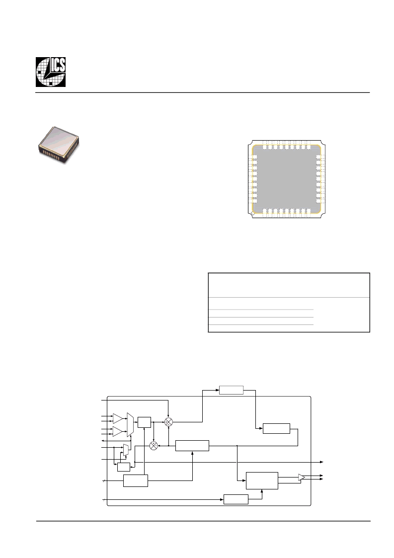
S
IMPLIFIED
B
LOCK
D
IAGRAM
P
IN
A
SSIGNMENT
(9 x 9 mm SMT)
Figure 1: Pin Assignment
Figure 2: Simplified Block Diagram
Example I/O Clock Frequency Combinations
Using
M1025-11-155.5200 or M1026-11-155.5200
Input Reference
Clock (MHz)
PLL Ratio
(Pin Selectable)
Output Clock
(MHz)
(Pin Selectable)
(M1025) (M1026)
19.44 or 38.88
77.76
155.52
622.08
(M1025) (M1026)
8 or 4
2
1
0.25
155.52
or
77.76
Table 1: Example I/O Clock Frequency Combinations
M1025
M1026
(Top View)
18
17
16
15
14
13
12
11
10
28
29
30
31
32
33
34
35
36
1
2
3
4
5
6
7
8
9
M
G
N
D
n
R
D
n
V
P_SEL0
P_SEL1
nFOUT
FOUT
GND
REF_ACK
AUTO
VCC
GND
MR_SEL2
MR_SEL0
MR_SEL1
LOL
NBW
VCC
DNC
DNC
DNC
n
O
V
n
n
O
G
G
G
1
2
2
2
2
2
2
2
2
FOUT
nFOUT
TriState
Loop Filter
PLL
Phase
Detector
R Div
MUX
0
REF_SEL
DIF_REF0
nDIF_REF0
1
P_SEL1:0
NBW
DIF_REF1
nDIF_REF1
Auto
Ref Sel
0
1
LOL
Phase
Detector
REF_ACK
AUTO
M1025/26
VCSO
P Divider
LUT
LOL
2
M Divider
4
M/R
Divider
LUT
MR_SEL3:0
P Divider
(1, 2, or TriState)
相關PDF資料 |
PDF描述 |
|---|---|
| M14C04 | Memory Card IC 16/4 Kbit Serial IC Bus EEPROM |
| M14C04DD | M14C04 Die Description |
| M14C32 | Memory Micromodules General Information for D1, D2 and C Packaging |
| M14C32DD | TERMINAL BLOCK, 8WAY; Connector type:Terminal Block, Barrier; Material, contact:Copper alloy; Plating, contact:Bright Tin; Positions, No. of:8; Pitch:0.375"; Mounting type:PC Board; Wire size, AWG:12AWG; Approval Bodies:UL, CSA; RoHS Compliant: Yes |
| M14C64 | Memory Card IC 64/32 Kbit Serial IC Bus EEPROM |
相關代理商/技術參數(shù) |
參數(shù)描述 |
|---|---|
| M1026-1Z-172.6423 | 制造商:ICS 制造商全稱:ICS 功能描述:VCSO BASED CLOCK PLL WITH AUTOSWITCH |
| M1026-1Z-173.3708 | 制造商:ICS 制造商全稱:ICS 功能描述:VCSO BASED CLOCK PLL WITH AUTOSWITCH |
| M10264-A1 | 功能描述:GPS模塊 GPS RF Ant Mod SiRF starIII Planar Mount RoHS:否 制造商:Linx Technologies 頻帶:1.575 GHz 通道數(shù)量:20 首次定位時間(冷啟動):35 s 獲取敏感性:- 144 dBm 水平位置精確度:10 m 工作電源電壓:3 V to 4.2 V 工作電源電流:46 mA 接口類型:Serial 最大工作溫度:+ 85 C 安裝風格:SMD/SMT 尺寸:15 mm x 13 mm x 2.2 mm |
| M10264-K1 | 功能描述:GPS開發(fā)工具 Evaluation Kit for M10214-A1 2 Modules RoHS:否 制造商:STMicroelectronics 產品:Evaluation Boards 工具用于評估:IT600, STM32F20x 頻率:1.575 GHz 工作電源電壓:1.8 V 接口類型:Wireless |
| M1026KS-6C-MMR | 制造商:MISCELLANEOUS 功能描述: |
發(fā)布緊急采購,3分鐘左右您將得到回復。