- 您現(xiàn)在的位置:買賣IC網(wǎng) > PDF目錄377801 > M12L64322A-6TG (ELITE SEMICONDUCTOR MEMORY TECHNOLOGY INC) 512K x 32 Bit x 4 Banks Synchronous DRAM PDF資料下載
參數(shù)資料
| 型號(hào): | M12L64322A-6TG |
| 廠商: | ELITE SEMICONDUCTOR MEMORY TECHNOLOGY INC |
| 元件分類: | DRAM |
| 英文描述: | 512K x 32 Bit x 4 Banks Synchronous DRAM |
| 中文描述: | 2M X 32 SYNCHRONOUS DRAM, 5.5 ns, PDSO86 |
| 封裝: | 0.400 X 0.875 INCH, 0.50 MM PITCH, LEAD FREE, TSOP2-86 |
| 文件頁數(shù): | 5/47頁 |
| 文件大?。?/td> | 791K |
| 代理商: | M12L64322A-6TG |
第1頁第2頁第3頁第4頁當(dāng)前第5頁第6頁第7頁第8頁第9頁第10頁第11頁第12頁第13頁第14頁第15頁第16頁第17頁第18頁第19頁第20頁第21頁第22頁第23頁第24頁第25頁第26頁第27頁第28頁第29頁第30頁第31頁第32頁第33頁第34頁第35頁第36頁第37頁第38頁第39頁第40頁第41頁第42頁第43頁第44頁第45頁第46頁第47頁
ES MT
M12L64322A
Elite Semiconductor Memory Technology Inc.
Publication Date: Mar. 2007
Revision
:
2.3
5/47
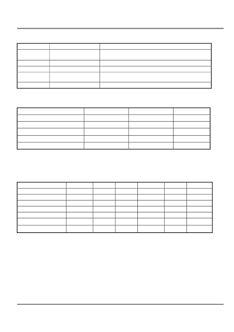
PIN
NAME
INPUT FUNCTION
DQM0~3
Data Input / Output Mask
Makes data output Hi-Z, t
SHZ
after the clock and masks the output.
Blocks data input when DQM active.
DQ0 ~ DQ31
Data Input / Output
Data inputs / outputs are multiplexed on the same pins.
V
DD
/ V
SS
Power Supply / Ground
Power and ground for the input buffers and the core logic.
V
DDQ
/ V
SSQ
Data Output Power / Ground
Isolated power supply and ground for the output buffers to provide
improved noise immunity.
N.C
No Connection
This pin is recommended to be left No Connection on the device.
ABSOLUTE MAXIMUM RATINGS
Parameter
Symbol
Value
Unit
Voltage on any pin relative to V
SS
V
IN
, V
OUT
-1.0 ~ 4.6
V
Voltage on V
DD
supply relative to V
SS
V
DD
, V
DDQ
-1.0 ~ 4.6
V
Storage temperature
T
STG
-55 ~ +150
C
°
Power dissipation
P
D
1
W
Short circuit current
Note :
Permanent device damage may occur if ABSOLUTE MAXIMUM RATING are exceeded.
Functional operation should be restricted to recommended operating condition.
Exposure to higher than recommended voltage for extended periods of time could affect device reliability.
DC OPERATING CONDITION
Recommended operating conditions (Voltage referenced to V
SS
= 0V, T
A
= 0 to 70° )
I
OS
50
mA
Parameter
Symbol
Min
Typ
Max
Unit
Note
Supply voltage
V
DD
, V
DDQ
3.0
3.3
3.6
V
Input logic high voltage
V
IH
2.0
3.0
V
DD
+0.3
V
1
Input logic low voltage
V
IL
-0.3
0
0.8
V
2
Output logic high voltage
V
OH
2.4
-
-
V
I
OH
= -2mA
Output logic low voltage
V
OL
-
-
0.4
V
μ
A
I
OL
= 2mA
Input leakage current
I
IL
-5
-
5
3
Output leakage current
I
OL
-5
-
5
μ
A
4
Note:
1. V
IH
(max) = 4.6V AC for pulse width
≤
10ns acceptable.
4. Dout is disabled , 0V
≤
V
OUT
≤
V
DD
.
2. V
IL
(min) = -1.5V AC for pulse width
≤
10ns acceptable.
3. Any input 0V
≤
VIN
≤
V
DD
+ 0.3V, all other pins are not under test = 0V.
相關(guān)PDF資料 |
PDF描述 |
|---|---|
| M12L64322A-7BG | 512K x 32 Bit x 4 Banks Synchronous DRAM |
| M12L64322A-7TG | 512K x 32 Bit x 4 Banks Synchronous DRAM |
| M12S128168A | 2M x 16 Bit x 4 Banks Synchronous DRAM |
| M12S128168A-10TG | 2M x 16 Bit x 4 Banks Synchronous DRAM |
| M12S16161A-7BG | 512K x 16Bit x 2Banks Synchronous DRAM |
相關(guān)代理商/技術(shù)參數(shù) |
參數(shù)描述 |
|---|---|
| M12L64322A-6TG2U | 制造商:ESMT 制造商全稱:Elite Semiconductor Memory Technology Inc. 功能描述:512K x 32 Bit x 4 Banks |
| M12L64322A-6TIG | 制造商:ESMT 制造商全稱:Elite Semiconductor Memory Technology Inc. 功能描述:512K x 32 Bit x 4 Banks Synchronous DRAM |
| M12L64322A-7BG | 制造商:ESMT 制造商全稱:Elite Semiconductor Memory Technology Inc. 功能描述:512K x 32 Bit x 4 Banks Synchronous DRAM |
| M12L64322A-7BG2U | 制造商:ESMT 制造商全稱:Elite Semiconductor Memory Technology Inc. 功能描述:512K x 32 Bit x 4 Banks |
| M12L64322A-7T | 制造商:未知廠家 制造商全稱:未知廠家 功能描述:512K x 32 Bit x 4 Banks Synchronous DRAM |
發(fā)布緊急采購,3分鐘左右您將得到回復(fù)。