- 您現(xiàn)在的位置:買賣IC網(wǎng) > PDF目錄377802 > M25PE10-VMN6G (意法半導(dǎo)體) 4 Mbit Uniform Sector, Serial Flash Memory PDF資料下載
參數(shù)資料
| 型號: | M25PE10-VMN6G |
| 廠商: | 意法半導(dǎo)體 |
| 元件分類: | DRAM |
| 英文描述: | 4 Mbit Uniform Sector, Serial Flash Memory |
| 中文描述: | 4兆位統(tǒng)一部門,串行閃存 |
| 文件頁數(shù): | 28/60頁 |
| 文件大小: | 310K |
| 代理商: | M25PE10-VMN6G |
第1頁第2頁第3頁第4頁第5頁第6頁第7頁第8頁第9頁第10頁第11頁第12頁第13頁第14頁第15頁第16頁第17頁第18頁第19頁第20頁第21頁第22頁第23頁第24頁第25頁第26頁第27頁當(dāng)前第28頁第29頁第30頁第31頁第32頁第33頁第34頁第35頁第36頁第37頁第38頁第39頁第40頁第41頁第42頁第43頁第44頁第45頁第46頁第47頁第48頁第49頁第50頁第51頁第52頁第53頁第54頁第55頁第56頁第57頁第58頁第59頁第60頁
Instructions
M25PE20, M25PE10
28/60
6.5
Write Status Register (WRSR)
The Write Status Register (WRSR) instruction allows new values to be written to the Status
Register.
Note:
The Status Register BPi and SRWD bits are available in the T9HX process only. See
Important note on page 6
for more details.
Before the Write Status Register (WRSR) instruction can be accepted, a Write Enable
(WREN) instruction must previously have been executed. After the Write Enable (WREN)
instruction has been decoded and executed, the device sets the Write Enable Latch (WEL).
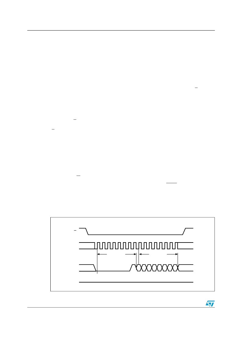
The Write Status Register (WRSR) instruction is entered by driving Chip Select (S) Low,
followed by the instruction code and the data byte on Serial Data Input (D).
The instruction sequence is shown in
Figure 12
.
The Write Status Register (WRSR) instruction has no effect on b6, b5, b1 and b0 of the
Status Register. b6 and b5 are always read as 0.
Chip Select (S) must be driven High after the eighth bit of the data byte has been latched in.
If not, the Write Status Register (WRSR) instruction is not executed. As soon as Chip Select
(S) is driven High, the self-timed Write Status Register cycle (whose duration is t
W
) is
initiated. While the Write Status Register cycle is in progress, the Status Register may still
be read to check the value of the Write In Progress (WIP) bit. The Write In Progress (WIP)
bit is 1 during the self-timed Write Status Register cycle, and is 0 when it is completed.
When the cycle is completed, the Write Enable Latch (WEL) is reset.
The Write Status Register (WRSR) instruction allows the user to change the values of the
Block Protect (BP1, BP0) bits, to define the size of the area that is to be treated as read-
only, as defined in
Table 3
. The Write Status Register (WRSR) instruction also allows the
user to set or reset the Status Register Write Disable (SRWD) bit in accordance with the
Write Protect (W) signal (see
Section 6.4.4
).
If a Write Status Register (WRSR) instruction is interrupted by a Reset Low pulse, the
internal cycle of the Write Status Register operation (whose duration is t
W
) is first completed
(provided that the supply voltage V
CC
remains within the operating range). After that the
device enters the Reset mode (see also
Table 14: Device status after a Reset Low pulse
and
Table 24: Timings after a Reset Low pulse
).
Figure 12.
Write Status Register (WRSR) instruction sequence
C
D
AI02282D
S
Q
2
1
3
4
5
6
7
8
9 10 11 12 13 14 15
High Impedance
Instruction
Status
Register In
0
7
6
5
4
3
2
0
1
MSB
相關(guān)PDF資料 |
PDF描述 |
|---|---|
| M25PE20-VMP6TP | 4 Mbit Uniform Sector, Serial Flash Memory |
| M25PE10-VMN6P | 4 Mbit Uniform Sector, Serial Flash Memory |
| M25PE10-VMP6G | 4 Mbit Uniform Sector, Serial Flash Memory |
| M25PE10-VMP6P | 4 Mbit Uniform Sector, Serial Flash Memory |
| M25PE10-VMP6TG | 4 Mbit Uniform Sector, Serial Flash Memory |
相關(guān)代理商/技術(shù)參數(shù) |
參數(shù)描述 |
|---|---|
| M25PE10-VMN6P | 功能描述:閃存 SERIAL PAGE ERASE FLASH 1MBIT DATAS RoHS:否 制造商:ON Semiconductor 數(shù)據(jù)總線寬度:1 bit 存儲類型:Flash 存儲容量:2 MB 結(jié)構(gòu):256 K x 8 定時類型: 接口類型:SPI 訪問時間: 電源電壓-最大:3.6 V 電源電壓-最小:2.3 V 最大工作電流:15 mA 工作溫度:- 40 C to + 85 C 安裝風(fēng)格:SMD/SMT 封裝 / 箱體: 封裝:Reel |
| M25PE10-VMN6TG | 制造商:NUMONYX 制造商全稱:Numonyx B.V 功能描述:1 and 2 Mbit, page-erasable serial Flash memories with byte alterability, 75 MHz SPI bus, standard pinout |
| M25PE10-VMN6TP | 功能描述:電可擦除可編程只讀存儲器 SERIAL PAGE ERASE FLASH 1 Mbit Datas RoHS:否 制造商:Atmel 存儲容量:2 Kbit 組織:256 B x 8 數(shù)據(jù)保留:100 yr 最大時鐘頻率:1000 KHz 最大工作電流:6 uA 工作電源電壓:1.7 V to 5.5 V 最大工作溫度:+ 85 C 安裝風(fēng)格:SMD/SMT 封裝 / 箱體:SOIC-8 |
| M25PE10-VMN6TPBA | 制造商:Micron Technology Inc 功能描述:SERIAL NOR 制造商:Micron Technology Inc 功能描述:NOR Flash Serial-SPI 3V/3.3V 1Mbit 128K x 8bit 8ns T/R 制造商:Micron Technology Inc 功能描述:AUTOMOTIVE - Tape and Reel |
| M25PE10-VMN6TPBA TR | 制造商:Micron Technology Inc 功能描述:IC FLASH 1MBIT 75MHZ 8SO |
發(fā)布緊急采購,3分鐘左右您將得到回復(fù)。