- 您現(xiàn)在的位置:買賣IC網(wǎng) > PDF目錄69008 > M30218MC-XXXXFP 16-BIT, MROM, 10 MHz, MICROCONTROLLER, PQFP100 PDF資料下載
參數(shù)資料
| 型號(hào): | M30218MC-XXXXFP |
| 元件分類: | 微控制器/微處理器 |
| 英文描述: | 16-BIT, MROM, 10 MHz, MICROCONTROLLER, PQFP100 |
| 封裝: | PLASTIC, QFP-100 |
| 文件頁(yè)數(shù): | 113/161頁(yè) |
| 文件大小: | 2043K |
| 代理商: | M30218MC-XXXXFP |
第1頁(yè)第2頁(yè)第3頁(yè)第4頁(yè)第5頁(yè)第6頁(yè)第7頁(yè)第8頁(yè)第9頁(yè)第10頁(yè)第11頁(yè)第12頁(yè)第13頁(yè)第14頁(yè)第15頁(yè)第16頁(yè)第17頁(yè)第18頁(yè)第19頁(yè)第20頁(yè)第21頁(yè)第22頁(yè)第23頁(yè)第24頁(yè)第25頁(yè)第26頁(yè)第27頁(yè)第28頁(yè)第29頁(yè)第30頁(yè)第31頁(yè)第32頁(yè)第33頁(yè)第34頁(yè)第35頁(yè)第36頁(yè)第37頁(yè)第38頁(yè)第39頁(yè)第40頁(yè)第41頁(yè)第42頁(yè)第43頁(yè)第44頁(yè)第45頁(yè)第46頁(yè)第47頁(yè)第48頁(yè)第49頁(yè)第50頁(yè)第51頁(yè)第52頁(yè)第53頁(yè)第54頁(yè)第55頁(yè)第56頁(yè)第57頁(yè)第58頁(yè)第59頁(yè)第60頁(yè)第61頁(yè)第62頁(yè)第63頁(yè)第64頁(yè)第65頁(yè)第66頁(yè)第67頁(yè)第68頁(yè)第69頁(yè)第70頁(yè)第71頁(yè)第72頁(yè)第73頁(yè)第74頁(yè)第75頁(yè)第76頁(yè)第77頁(yè)第78頁(yè)第79頁(yè)第80頁(yè)第81頁(yè)第82頁(yè)第83頁(yè)第84頁(yè)第85頁(yè)第86頁(yè)第87頁(yè)第88頁(yè)第89頁(yè)第90頁(yè)第91頁(yè)第92頁(yè)第93頁(yè)第94頁(yè)第95頁(yè)第96頁(yè)第97頁(yè)第98頁(yè)第99頁(yè)第100頁(yè)第101頁(yè)第102頁(yè)第103頁(yè)第104頁(yè)第105頁(yè)第106頁(yè)第107頁(yè)第108頁(yè)第109頁(yè)第110頁(yè)第111頁(yè)第112頁(yè)當(dāng)前第113頁(yè)第114頁(yè)第115頁(yè)第116頁(yè)第117頁(yè)第118頁(yè)第119頁(yè)第120頁(yè)第121頁(yè)第122頁(yè)第123頁(yè)第124頁(yè)第125頁(yè)第126頁(yè)第127頁(yè)第128頁(yè)第129頁(yè)第130頁(yè)第131頁(yè)第132頁(yè)第133頁(yè)第134頁(yè)第135頁(yè)第136頁(yè)第137頁(yè)第138頁(yè)第139頁(yè)第140頁(yè)第141頁(yè)第142頁(yè)第143頁(yè)第144頁(yè)第145頁(yè)第146頁(yè)第147頁(yè)第148頁(yè)第149頁(yè)第150頁(yè)第151頁(yè)第152頁(yè)第153頁(yè)第154頁(yè)第155頁(yè)第156頁(yè)第157頁(yè)第158頁(yè)第159頁(yè)第160頁(yè)第161頁(yè)
55
Under
development
Tentative Specifications REV.A1
Specifications in this manual are tentative and subject to change.
Mitsubishi microcomputers
M30218 Group
SINGLE-CHIP 16-BIT CMOS MICROCOMPUTER
FLD controller
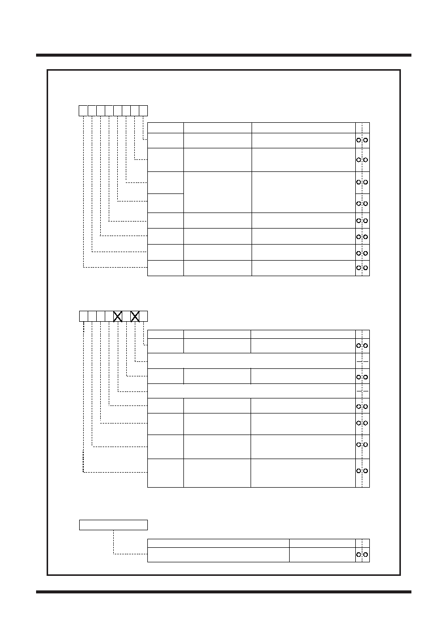
Figure KA-2. FLDC-related Register(1)
FLDC mode register
SymbolAddressWhen reset
FLDM035016
0016
Bit nameFunction
Bit symbol
b7b6b5b4b3b2b1b0
Automatic display
control bit
0 : General-purpose mode
1 : Automatic display mode
FLDM0
FLDM1
FLDM2
FLDM3
Display start bit0 : Stop display
1 : Display
(start to display by switching “0” to “1”)
Tscan control bits
00 : FLD digit interrupt
(at rising edge of each digit)
01 : 1 X Tdisp
10 : 2 X Tdisp
11 : 3 X Tdisp
0 : 16 timing mode
1 : 32 timing mode
Timing number control bit
Gradation display mode
selection control bit
0 : Not selecting
1 : Selecting (Note )
FLDM4
FLDM5
Note : When a gradation display mode is selected, a number of timing is max. 16 timing.
(Set the timing number control bit to “0”.)
Tdisp counter
count source selection bit
0 : f(XIN)/32
1 : f(XIN)/128
FLDM6
High-breakdown voltage
port drivability select bit
0 : Drivability strong
1 : Drivability weak
FLDM7
FLD output control register
SymbolAddressWhen reset
FLDCON035116
0016
Bit nameFunction
Bit symbol
b7b6b5b4b3b2b1b0
FLDCON7
FLDCON5
FLDCON4
FLDCON2
FLDCON0
FLDCON6
P44 to P47 FLD
output reverse bit
P44 to P47 FLD
Toff is invalid bit
0 : Perform normally
1 : Toff is invalid
P97 dimmer output
control bit
0 : Output normally
1 : Dimmer output
CMOS ports: section of
Toff generate/not
generate bit
0 : section of Toff does NOT generate
1 : section of Toff generates
High-breakdown-voltage ports:
section of Toff
generate/not generate bit
0 : section of Toff does NOT generate
1 : section of Toff generates
Toff2
SET/RESET change bit
0 : gradation display data is reset at Toff2
(set at Toff1)
1 : gradation display data is set at Toff2
(reset at Toff1)
W
R
0 : Output normally
1 : Reverse output
Nothing is assigned.
In an attempt to write to this bit, write “0”. The value, if read, turns out to be “0”.
Nothing is assigned.
In an attempt to write to this bit, write “0”. The value, if read, turns out to be “0”.
Tdisp time set register
SymbolAddressWhen reset
TDISP035216
0016
Values that can be set
b7b0
Counts Tdisp time. Count source is selected by Tdisp
counter count source select bit.
W
R
016 to FF16
Function
FLD blanking
interrupt (at falling
edge of last digit)
}
b3b2
W
R
相關(guān)PDF資料 |
PDF描述 |
|---|---|
| M30218MFCFP | 16-BIT, FLASH, 10 MHz, MICROCONTROLLER, PQFP100 |
| M30220FCRP | 16-BIT, FLASH, 10 MHz, MICROCONTROLLER, PQFP144 |
| M30220MA-XXXGP | 16-BIT, MROM, 10 MHz, MICROCONTROLLER, PQFP144 |
| M30220MA-XXXRP | 16-BIT, MROM, 10 MHz, MICROCONTROLLER, PQFP144 |
| M30220FCRP | 16-BIT, FLASH, 10 MHz, MICROCONTROLLER, PQFP144 |
相關(guān)代理商/技術(shù)參數(shù) |
參數(shù)描述 |
|---|---|
| M3021E8F2-AXXXFP | 制造商:RENESAS 制造商全稱:Renesas Technology Corp 功能描述:SINGLE-CHIP 16-BIT CMOS MICROCOMPUTER |
| M3021E8F4-AXXXFP | 制造商:RENESAS 制造商全稱:Renesas Technology Corp 功能描述:SINGLE-CHIP 16-BIT CMOS MICROCOMPUTER |
| M3021E8F6-AXXXFP | 制造商:RENESAS 制造商全稱:Renesas Technology Corp 功能描述:SINGLE-CHIP 16-BIT CMOS MICROCOMPUTER |
| M3021E8F8-AXXXFP | 制造商:RENESAS 制造商全稱:Renesas Technology Corp 功能描述:SINGLE-CHIP 16-BIT CMOS MICROCOMPUTER |
| M3021E8FA-AXXXFP | 制造商:RENESAS 制造商全稱:Renesas Technology Corp 功能描述:SINGLE-CHIP 16-BIT CMOS MICROCOMPUTER |
發(fā)布緊急采購(gòu),3分鐘左右您將得到回復(fù)。