- 您現(xiàn)在的位置:買賣IC網 > PDF目錄224185 > M95020-RDW3TP/W (STMICROELECTRONICS) 256 X 8 SPI BUS SERIAL EEPROM, PDSO8 PDF資料下載
參數(shù)資料
| 型號: | M95020-RDW3TP/W |
| 廠商: | STMICROELECTRONICS |
| 元件分類: | PROM |
| 英文描述: | 256 X 8 SPI BUS SERIAL EEPROM, PDSO8 |
| 封裝: | 0.169 INCH, ROHS COMPLIANT, TSSOP-8 |
| 文件頁數(shù): | 15/42頁 |
| 文件大小: | 250K |
| 代理商: | M95020-RDW3TP/W |
第1頁第2頁第3頁第4頁第5頁第6頁第7頁第8頁第9頁第10頁第11頁第12頁第13頁第14頁當前第15頁第16頁第17頁第18頁第19頁第20頁第21頁第22頁第23頁第24頁第25頁第26頁第27頁第28頁第29頁第30頁第31頁第32頁第33頁第34頁第35頁第36頁第37頁第38頁第39頁第40頁第41頁第42頁
Instructions
M95040, M95020, M95010
6.6
Write to Memory Array (WRITE)
As shown in Figure 12, to send this instruction to the device, Chip Select (S) is first driven
Low. The bits of the instruction byte, address byte, and at least one data byte are then
shifted in, on Serial Data Input (D).
The instruction is terminated by driving Chip Select (S) High after the rising edge of Serial
Clock (C) that latches the last data bit, and before the next rising edge of Serial Clock (C)
occurs anywhere on the bus. In the case of Figure 12, this occurs after the eighth bit of the
data byte has been latched in, indicating that the instruction is being used to write a single
byte. The self-timed Write cycle starts, and continues for a period tWC (as specified in
If, though, Chip Select (S) continues to be driven Low, as shown in Figure 13, the next byte
of input data is shifted in. In this way, all the bytes from the given address to the end of the
same page can be programmed in a single instruction.
If Chip Select (S) still continues to be driven Low, the next byte of input data is shifted in, and
is used to overwrite the byte at the start of the current page.
The instruction is not accepted, and is not executed, under the following conditions:
●
if the Write Enable Latch (WEL) bit has not been set to 1 (by executing a Write Enable
instruction just before)
●
if a Write cycle is already in progress
●
if the device has not been deselected, by Chip Select (S) being driven High, at a byte
boundary (after the rising edge of Serial Clock (C) that latches the last data bit, and
before the next rising edge of Serial Clock (C) occurs anywhere on the bus)
●
if Write Protect (W) is Low or if the addressed page is in the region protected by the
Block Protect (BP1 and BP0) bits.
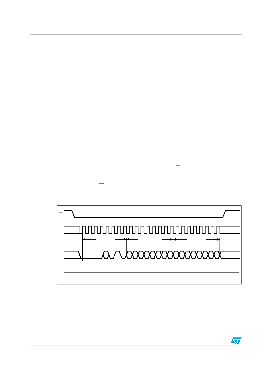
Figure 12.
Byte Write (WRITE) sequence
1.
Depending on the memory size, as shown in Table 6, the most significant address bits are Don’t Care.
AI01442D
C
D
S
Q
A7
2
1
3456789 10 11 12 13 14 15 16 17 18 19
A6 A5 A4 A3 A2 A1 A0
A8
20 21 22 23
High Impedance
Instruction
Byte Address
0
765432
0
1
Data Byte
相關PDF資料 |
PDF描述 |
|---|---|
| M95020-WMN3G/W | 256 X 8 SPI BUS SERIAL EEPROM, PDSO8 |
| M95256-RDW3/A | 32K X 8 SPI BUS SERIAL EEPROM, PDSO8 |
| M95256-RMN6P/A | 32K X 8 SPI BUS SERIAL EEPROM, PDSO8 |
| M95256-WDW3T/A | 32K X 8 SPI BUS SERIAL EEPROM, PDSO8 |
| M95256-RDW6TG | 32K X 8 SPI BUS SERIAL EEPROM, PDSO8 |
相關代理商/技術參數(shù) |
參數(shù)描述 |
|---|---|
| M95020-RDW6 | 制造商:STMICROELECTRONICS 制造商全稱:STMicroelectronics 功能描述:4Kbit, 2Kbit and 1Kbit Serial SPI Bus EEPROM With High Speed Clock |
| M95020-RDW6/W | 制造商:STMICROELECTRONICS 制造商全稱:STMicroelectronics 功能描述:4Kbit, 2Kbit and 1Kbit Serial SPI Bus EEPROM With High Speed Clock |
| M95020-RDW6G | 制造商:STMICROELECTRONICS 制造商全稱:STMicroelectronics 功能描述:4Kbit, 2Kbit and 1Kbit Serial SPI Bus EEPROM With High Speed Clock |
| M95020-RDW6G/W | 制造商:STMICROELECTRONICS 制造商全稱:STMicroelectronics 功能描述:4Kbit, 2Kbit and 1Kbit Serial SPI Bus EEPROM With High Speed Clock |
| M95020-RDW6P | 制造商:STMICROELECTRONICS 制造商全稱:STMicroelectronics 功能描述:4Kbit, 2Kbit and 1Kbit Serial SPI Bus EEPROM With High Speed Clock |
發(fā)布緊急采購,3分鐘左右您將得到回復。