- 您現(xiàn)在的位置:買賣IC網(wǎng) > PDF目錄383540 > MAX9222ETM (MAXIM INTEGRATED PRODUCTS INC) Programmable DC-Balance 21-Bit Deserializers PDF資料下載
參數(shù)資料
| 型號(hào): | MAX9222ETM |
| 廠商: | MAXIM INTEGRATED PRODUCTS INC |
| 元件分類: | 通用總線功能 |
| 英文描述: | Programmable DC-Balance 21-Bit Deserializers |
| 中文描述: | QUAD LINE RECEIVER, PQCC48 |
| 封裝: | 7 X 7 MM, 0.80 MM HEIGHT, MO-220, TQFN-48 |
| 文件頁(yè)數(shù): | 13/18頁(yè) |
| 文件大小: | 904K |
| 代理商: | MAX9222ETM |
第1頁(yè)第2頁(yè)第3頁(yè)第4頁(yè)第5頁(yè)第6頁(yè)第7頁(yè)第8頁(yè)第9頁(yè)第10頁(yè)第11頁(yè)第12頁(yè)當(dāng)前第13頁(yè)第14頁(yè)第15頁(yè)第16頁(yè)第17頁(yè)第18頁(yè)
M
Programmable DC-Balance
21-Bit Deserializers
______________________________________________________________________________________
13
bias resistors, along with the 100
±1% tolerance ter-
mination resistor, provide +15mV of differential input.
However, the +15mV bias causes degradation of
RSKM proportional to the slew rate of the clock input.
For example, if the clock transitions 250mV in 500ps,
the slew rate of 0.5mV/ps reduces RSKM by 30ps.
Unused LVDS Data Inputs
In non-DC-balanced mode, leave unused LVDS data
inputs open. In non-DC balanced mode, the input fail-
safe circuit drives the corresponding outputs low and no
pullup or pulldown resistors are needed. In DC-balanced
mode, at each unused LVDS data input, pull the inverting
input up to V
CC
using a 10k
resistor, and pull the nonin-
verting input down to ground using a 10k
resistor. Do
not connect a termination resistor. The pullup and pull-
down resistors drive the corresponding outputs low and
prevent switching due to noise.
PWRDWN
Driving
PWRDWN
low puts the outputs in high imped-
ance, stops the PLL, and reduces supply current to
50μA or less. Driving
PWRDWN
high drives the outputs
low until the PLL locks. The outputs of two deserializers
can be bused to form a 2:1 mux with the outputs con-
trolled by
PWRDWN
. Wait 100ns between disabling one
deserializer (driving
PWRDWN
low) and enabling the
second one (driving
PWRDWN
high) to avoid con-
tention of the bused outputs.
Input Clock and PLL Lock Time
There is no required timing sequence for the applica-
tion or reapplication of the parallel rate clock (RxCLK
IN) relative to
PWRDWN
, or to a power-supply ramp for
proper PLL lock. The PLL lock time is set by an internal
counter. The maximum time to lock is 32,800 clock
periods. Power and clock should be stable to meet the
lock time specification. When the PLL is locking, the
outputs are low.
Power-Supply Bypassing
There are separate on-chip power domains for digital
circuits, outputs, PLL, and LVDS inputs. Bypass each
V
CC
, V
CCO
, PLL V
CC
, and LVDS V
CC
pin with high-fre-
quency, surface-mount ceramic 0.1μF and 0.001μF
capacitors in parallel as close to the device as possi-
ble, with the smallest value capacitor closest to the
supply pin.
Cables and Connectors
Interconnect for LVDS typically has a differential imped-
ance of 100
. Use cables and connectors that have
matched differential impedance to minimize impedance
discontinuities.
Twisted-pair and shielded twisted-pair cables offer
superior signal quality compared to ribbon cable and
tend to generate less EMI due to magnetic field cancel-
ing effects. Balanced cables pick up noise as common
mode, which is rejected by the LVDS receiver.
Board Layout
Keep the LVTTL/LVCMOS outputs and LVDS input sig-
nals separated to prevent crosstalk. A four-layer PC
board with separate layers for power, ground, LVDS
inputs, and digital signals is recommended.
IEC 61000-4-2 Level 4 ESD Protection
The IEC 61000-4-2 standard specifies ESD tolerance
for electronic systems. The IEC 61000-4-2 model
(Figure 14) specifies a 150pF capacitor that is dis-
charged into the device through a 330
resistor. The
MAX9210/MAX9212/MAX9214/MAX9216/MAX9220/
MAX9222 LVDS inputs are rated for IEC 61000-4-2
level 4 (
±
8kV contact discharge and ±15kV air dis-
charge). IEC 61000-4-2 discharges higher peak current
and more energy than the HBM due to the lower series
resistance and larger capacitor. The HBM (Figure 15)
specifies a 100pF capacitor that is discharged into the
device through a 1.5k
resistor. All pins are rated for
±5kV HBM.
STORAGE
CAPACITOR
HIGH-
VOLTAGE
DC
SOURCE
DEVICE
UNDER
TEST
CHARGE-CURRENT-
LIMIT RESISTOR
DISCHARGE
RESISTANCE
R1
50
TO 100
R2
330k
C
S
150pF
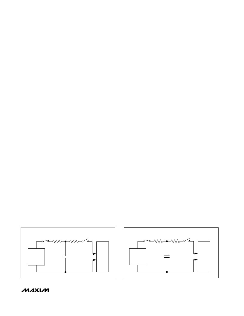
Figure 14. IEC 61000-4-2 Contact Discharge ESD Test Circuit
STORAGE
CAPACITOR
HIGH-
VOLTAGE
DC
SOURCE
DEVICE
UNDER
TEST
CHARGE-CURRENT-
LIMIT RESISTOR
DISCHARGE
RESISTANCE
R1
1M
R2
1.5k
C
S
100pF
Figure 15. Human Body ESD Test Circuit
相關(guān)PDF資料 |
PDF描述 |
|---|---|
| MAX9216ETM | Programmable DC-Balance 21-Bit Deserializers |
| MAX922CUA | Ultra Low-Power, Single/Dual-Supply Comparators |
| MAX921-MAX924 | Ultra Low-Power, Single/Dual-Supply Comparators |
| MAX922 | Ultra Low-Power, Single/Dual-Supply Comparators |
| MAX923 | Ultra Low-Power, Single/Dual-Supply Comparators |
相關(guān)代理商/技術(shù)參數(shù) |
參數(shù)描述 |
|---|---|
| MAX9222EUM | 制造商:MAXIM 制造商全稱:Maxim Integrated Products 功能描述:Programmable DC-Balance 21-Bit Deserializers |
| MAX9222EUM+ | 制造商:Maxim Integrated Products 功能描述:LVDS DESERLIZER 48TSSOP - Rail/Tube |
| MAX9222EUM+D | 制造商:Maxim Integrated Products 功能描述:LVDS DESERLIZER 48TSSOP - Rail/Tube |
| MAX9222EUM+T | 制造商:Maxim Integrated Products 功能描述:LVDS DESERLIZER 48TSSOP - Tape and Reel |
| MAX9222EUM+TD | 制造商:Maxim Integrated Products 功能描述:- Tape and Reel |
發(fā)布緊急采購(gòu),3分鐘左右您將得到回復(fù)。