- 您現(xiàn)在的位置:買賣IC網(wǎng) > PDF目錄377930 > MB90M407APF (FUJITSU LTD) 16-Bit Original Microcontroller PDF資料下載
參數(shù)資料
| 型號(hào): | MB90M407APF |
| 廠商: | FUJITSU LTD |
| 元件分類: | 微控制器/微處理器 |
| 英文描述: | 16-Bit Original Microcontroller |
| 中文描述: | 16-BIT, MROM, 16 MHz, MICROCONTROLLER, PQFP100 |
| 封裝: | 0.65 MM PITCH, PLASTIC, QFP-100 |
| 文件頁(yè)數(shù): | 51/64頁(yè) |
| 文件大?。?/td> | 310K |
| 代理商: | MB90M407APF |
第1頁(yè)第2頁(yè)第3頁(yè)第4頁(yè)第5頁(yè)第6頁(yè)第7頁(yè)第8頁(yè)第9頁(yè)第10頁(yè)第11頁(yè)第12頁(yè)第13頁(yè)第14頁(yè)第15頁(yè)第16頁(yè)第17頁(yè)第18頁(yè)第19頁(yè)第20頁(yè)第21頁(yè)第22頁(yè)第23頁(yè)第24頁(yè)第25頁(yè)第26頁(yè)第27頁(yè)第28頁(yè)第29頁(yè)第30頁(yè)第31頁(yè)第32頁(yè)第33頁(yè)第34頁(yè)第35頁(yè)第36頁(yè)第37頁(yè)第38頁(yè)第39頁(yè)第40頁(yè)第41頁(yè)第42頁(yè)第43頁(yè)第44頁(yè)第45頁(yè)第46頁(yè)第47頁(yè)第48頁(yè)第49頁(yè)第50頁(yè)當(dāng)前第51頁(yè)第52頁(yè)第53頁(yè)第54頁(yè)第55頁(yè)第56頁(yè)第57頁(yè)第58頁(yè)第59頁(yè)第60頁(yè)第61頁(yè)第62頁(yè)第63頁(yè)第64頁(yè)
MB90M405 Series
51
*6 : Corresponds to pins FIP0 to FIP59.
Note : V
CC
in the standard signifies V
DD
-FIP
=
V
CC
-CPU. Also, use the 3 pins on the left at the same power level.
Here, V
SS
signifies V
SS
-IO
=
V
SS
-CPU. Please connect this pin to GND as well.
WARNING:
Semiconductor devices can be permanently damaged by application of stress (voltage, current,
temperature, etc.) in excess of absolute maximum ratings. Do not exceed these ratings.
2.
Recommended Operating Conditions
(V
SS
-IO
=
V
SS
-CPU
=
AV
SS
=
0.0 V)
Note : V
CC
in the standard signifies V
DD
-FIP
=
V
CC
-CPU. Also, use the 3 pins on the left at the same power level.
Here, Vss signifies V
SS
-IO
=
V
SS
-CPU. Please connect this pin to GND as well.
WARNING:
The recommended operating conditions are required in order to ensure the normal operation of the
semiconductor device. All of the device’s electrical characteristics are warranted when the device is
operated within these ranges.
Always use semiconductor devices within their recommended operating condition ranges. Operation
outside these ranges may adversely affect reliability and could result in device failure.
No warranty is made with respect to uses, operating conditions, or combinations not represented on
the data sheet. Users considering application outside the listed conditions are advised to contact their
FUJITSU representatives beforehand.
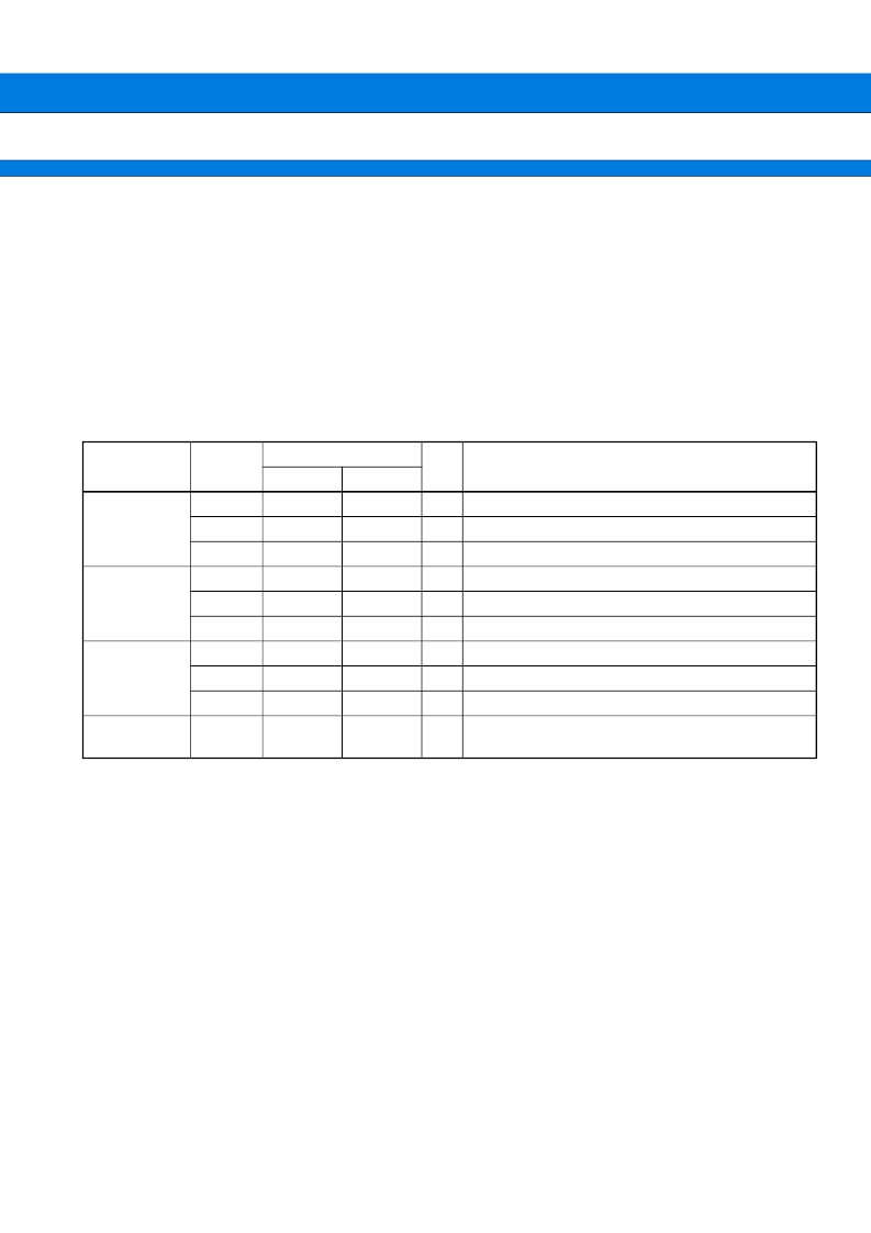
Parameter
Symbol
Values
Unit
Remarks
Min
Max
Power Voltage
V
CC
-CPU
3.0
3.6
V
During normal operation
V
DD
-FIP
3.0
3.6
V
During normal operation
V
CC
2.5
3.6
V
Save stop operation status
Input “H ” Volt-
age
V
HIS
0.8 V
CC
V
CC
+
0.3
V
SS
+
5.0
V
CC
+
0.3
0.2 V
CC
V
CMOS hysteresis input pin except I
2
C
V
HIS2
0.8 V
CC
V
CC
0.3
V
SS
0.3
V
SS
0.3
V
SS
0.3
V
I
2
C CMOS hysteresis input pin (5 V voltage resistant)
V
HIM
V
MD pin input
Input “ L” Volt-
age
V
ILS
V
CMOS hysteresis input pin except I
2
C
V
ILS2
0.2 V
CC
V
SS
+
0.3
V
I
2
C CMOS hysteresis input pin (5 V voltage resistant)
V
ILM
V
MD pin input
Operating
Temperature
Ta
40
+
85
°
C
相關(guān)PDF資料 |
PDF描述 |
|---|---|
| MB90M407PF | 16-Bit Original Microcontroller |
| MB90M408APF | 16-Bit Original Microcontroller |
| MB90M408PF | 16-Bit Original Microcontroller |
| MB90MF408APF | 16-Bit Original Microcontroller |
| MB90MF408PF | 16-Bit Original Microcontroller |
相關(guān)代理商/技術(shù)參數(shù) |
參數(shù)描述 |
|---|---|
| MB90V340A-102CR | 制造商:FUJITSU 功能描述: |
| MB-910 | 制造商:Circuit Test 功能描述:BREADBOARD WIRING KIT - 350 PCS |
| MB9100100 | 制造商:COM/DUO 功能描述:FAN 4-6WKS |
| MB9100-100 | 制造商:COM/DUO 功能描述:FAN 4-6WKS |
| MB91101 | 制造商:Panasonic Industrial Company 功能描述:IC |
發(fā)布緊急采購(gòu),3分鐘左右您將得到回復(fù)。