- 您現(xiàn)在的位置:買賣IC網(wǎng) > PDF目錄371003 > MC10E197FN (MOTOROLA INC) DATA SEPARATOR PDF資料下載
參數(shù)資料
| 型號: | MC10E197FN |
| 廠商: | MOTOROLA INC |
| 元件分類: | 光電元器件 |
| 英文描述: | DATA SEPARATOR |
| 中文描述: | PULSE DETECTOR, PQCC28 |
| 封裝: | PLASTIC, LCC-28 |
| 文件頁數(shù): | 8/16頁 |
| 文件大小: | 217K |
| 代理商: | MC10E197FN |

MC10E197
MOTOROLA
ECLinPS and ECLinPS Lite
DL140 — Rev 4
2–8
the poles lie beyond the crossover frequency and they are
positioned for near unity gain operation. Performing a root
locus analysis on the op-amp open loop configuration and
adhering to the two constraints yields the pole positions
contributed by the op-amp.
Determination of Element Values
Since the difference amplifier is configured to operate as a
differential summer the resistor values associated with the
amplifier are of equal value. Further, the typical input
resistance to the summing amplifier is 1k
; thus, the op-amp
resistors are set at 1 k
. Having set the input resistance to the
op-amp and selected the position of the real pole, the value of
the shunt capacitors is determined using the following
relationship:
p1
=
1
2
π
R1CIN
eqt. 4
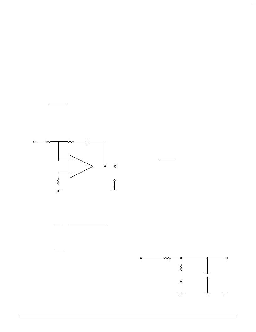
Augmenting Integrator
The augmenting integrator consists of an active filter with a
lag-lead network in the feedback path (Figure 7).
VIN
VCCVCO
MC34182
RIA
RA
CA
VO2
RIA
Figure 7. Integrator Subsection
Analysis of this portion of the filter circuit yields the transfer
function:
F1(s) = Kl *
1
s
*
(s + z)
[s2 + (2
ζω
ω
o2
) s +
The gain constant is defined as:
where:
Al =
op-amp gain constant for selected pole positions.
RA = integrator feedback resistor.
RlA = integrator input resistor.
Kl = Al *
RA
RlA
eqt. 5
The integrator circuit introduces a zero, a pole at the origin,
and a second order pole set as described by the two pole
model for an op-amp. As in the case of the differential
summing amplifier, we assume the op-amp pole pair occur as
a complex conjugate pair making an angle of 45
°
to the real
axis of the complex frequency plane; are positioned for near
unity gain operation; and are located beyond the crossover
frequency. Since both the summing and integrating op-amps
are realized by the same type of op-amp (MC34182D), the
open loop pole positions for both amplifiers will be the same.
Further, the loop transfer function contains two poles
located at the origin, one introduced by the integrator and the
other by the VCO; hence a zero is necessary to compensate
for the phase shift produced by these poles and ensure loop
stability. The op-amp will be stable if the crossover point
occurs before the transfer function phase angle becomes
180
°
. The zero should be positioned much less than one
decade before the unity gain frequency.
As in the case of the filter input circuitry, the poles and zero
from this analysis will be used as open loop poles and a zero
when performing the root locus analysis for the complete
system.
Determination of Element Values
The location of the zero is used to determine the element
values for the augmenting integrator. The value of the
capacitor, CA, is selected to provide adequate charge storage
when the loop is not sampling data. A value of 0.1
μ
F is
sufficient for most applications; this value may be increased
when the RDCLK frequency is much lower than 4 MHz. The
value of RA is governed by:
z
=
1
2
π
RACA
eqt. 6
For unity gain operation of the integrating op-amp the value of
RlA is selected such that:
RlA = RA
eqt. 7
It should be noted that although the zero can be tuned by
varying either RA or CA, caution must be exercised when
adjusting the zero by varying CA because the integrator gain is
also a function of CA. Further, the gain of the loop filter can be
adjusted by changing the integrator input resistor RlA.
Voltage Divider
The input range to the VCOIN input is from 1.3V + VEE to
2.6V + VEE; hence, the output from the augmenting amplifier
section must be attenuated to meet the VCOIN constraints. A
simple voltage divider network provides the necessary
attenuation (Figure 8).
VIN
RV
RO
DB
Cd
VO
Figure 8. Voltage Divider Subsection
相關PDF資料 |
PDF描述 |
|---|---|
| MC10E197 | DATA SEPARATOR |
| MC10EL32D | Dual 1A Current-Limited, Power-Distribution Switches 8-MSOP-PowerPAD -40 to 85 |
| MC10EL32 | Dual 1A Current-Limited, Power-Distribution Switches 8-SOIC -40 to 85 |
| MC100EL32D | ±2 Divider |
| MC10EL33D | ±4 Divider |
相關代理商/技術參數(shù) |
參數(shù)描述 |
|---|---|
| MC10E211 C14N WAF | 制造商:ON Semiconductor 功能描述: |
| MC10E211FN | 功能描述:時鐘驅動器及分配 5V ECL 1:6 Diff RoHS:否 制造商:Micrel 乘法/除法因子:1:4 輸出類型:Differential 最大輸出頻率:4.2 GHz 電源電壓-最大: 電源電壓-最小:5 V 最大工作溫度:+ 85 C 封裝 / 箱體:SOIC-8 封裝:Reel |
| MC10E211FNG | 功能描述:時鐘驅動器及分配 5V ECL 1:6 Diff Clock Driver RoHS:否 制造商:Micrel 乘法/除法因子:1:4 輸出類型:Differential 最大輸出頻率:4.2 GHz 電源電壓-最大: 電源電壓-最小:5 V 最大工作溫度:+ 85 C 封裝 / 箱體:SOIC-8 封裝:Reel |
| MC10E211FNR2 | 功能描述:時鐘驅動器及分配 5V ECL 1:6 Diff RoHS:否 制造商:Micrel 乘法/除法因子:1:4 輸出類型:Differential 最大輸出頻率:4.2 GHz 電源電壓-最大: 電源電壓-最小:5 V 最大工作溫度:+ 85 C 封裝 / 箱體:SOIC-8 封裝:Reel |
| MC10E211FNR2G | 功能描述:時鐘驅動器及分配 5V ECL 1:6 Diff Clock Driver RoHS:否 制造商:Micrel 乘法/除法因子:1:4 輸出類型:Differential 最大輸出頻率:4.2 GHz 電源電壓-最大: 電源電壓-最小:5 V 最大工作溫度:+ 85 C 封裝 / 箱體:SOIC-8 封裝:Reel |
發(fā)布緊急采購,3分鐘左右您將得到回復。