- 您現在的位置:買賣IC網 > PDF目錄371013 > MC145053D (MOTOROLA INC) -48V Hot Swap Controller 8-MSOP -40 to 85 PDF資料下載
參數資料
| 型號: | MC145053D |
| 廠商: | MOTOROLA INC |
| 元件分類: | ADC |
| 英文描述: | -48V Hot Swap Controller 8-MSOP -40 to 85 |
| 中文描述: | 5-CH 10-BIT SUCCESSIVE APPROXIMATION ADC, SERIAL ACCESS, PDSO14 |
| 封裝: | SOG-14 |
| 文件頁數: | 4/15頁 |
| 文件大小: | 166K |
| 代理商: | MC145053D |
MC145053
4
MOTOROLA WIRELESS SEMICONDUCTOR
SOLUTIONS DEVICE DATA
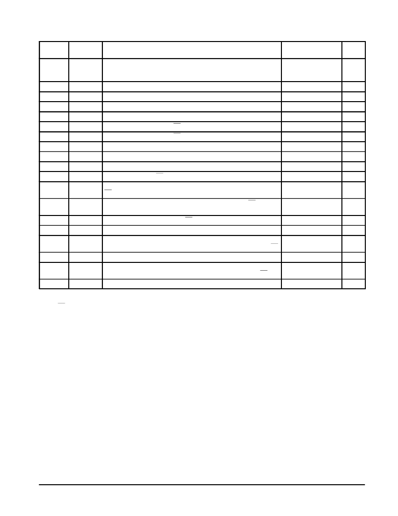
AC ELECTRICAL CHARACTERISTICS
(Full Temperature and Voltage Ranges per Operation Ranges Table)
Figure
Symbol
Parameter
Guaranteed
Limit
Unit
1
f
Clock Frequency, SCLK
(10-bit xfer) Min
(11- to 16-bit xfer) Min
(10- to 16-bit xfer) Max)
Note: Refer to twH, twL below
0
Note 1
2.1
MHz
1
twH
twL
Minimum Clock High Time, SCLK
190
ns
1
Minimum Clock Low Time, SCLK
190
ns
1, 7
tPLH, tPHL
th
tPLZ, tPHZ
tPZL, tPZH
tsu
th
td
tsu
tCSd
Maximum Propagation Delay, SCLK to Dout
Minimum Hold Time, SCLK to Dout
Maximum Propagation Delay, CS to Dout High-Z
Maximum Propagation Delay, CS to Dout Driven
Minimum Setup Time, Din to SCLK
Minimum Hold Time, SCLK to Din
Maximum Delay Time, EOC to Dout (MSB)
Minimum Setup Time, CS to SCLK
125
ns
1, 7
10
ns
2, 7
150
ns
2, 7
2.3
μ
s
3
100
ns
3
0
ns
4, 7, 8
100
ns
5
2.425
μ
s
—
Minimum Time Required Between 10th SCLK Falling Edge (
≤
0.8 V) and
CS to Allow a Conversion
Note 2
—
tCAs
Maximum Delay Between 10th SCLK Falling Edge (
≤
2 V) and CS to
Abort a Conversion
9
μ
s
5
th
Minimum Hold Time, Last SCLK to CS
0
ns
6, 8
tPHL
tr, tf
Maximum Propagation Delay, 10th SCLK to EOC
2.35
μ
s
1
Maximum Input Rise and Fall Times
SCLK
Din, CS
1
10
ms
μ
s
1, 4, 6 – 8
tTLH, tTHL
Cin
Maximum Output Transition Time, Any Output
300
ns
—
Maximum Input Capacitance
AN0 – AN4
SCLK, CS, Din
55
15
pF
—
Cout
Maximum Three-State Output Capacitance
Dout
15
pF
NOTES:
1. After the 10th SCLK falling edge (
≤
2 V), at least 1 SCLK rising edge (
≥
2 V) must occur within 18.5
μ
s.
2. A CS edge may be received immediately after an active transition on the EOC pin.
相關PDF資料 |
PDF描述 |
|---|---|
| MC145053P | -48V Hot Swap Controller 8-MSOP -40 to 85 |
| MC14506UBCL | Dual 2-Wide, 2-Input Expandable AND-OR-INVERT Gate |
| MC14506 | Dual 2-Wide, 2-Input Expandable AND-OR-INVERT Gate |
| MC14506UBCP | Dual 2-Wide, 2-Input Expandable AND-OR-INVERT Gate |
| MC14506UBD | Dual 2-Wide, 2-Input Expandable AND-OR-INVERT Gate |
相關代理商/技術參數 |
參數描述 |
|---|---|
| MC14508BBJBS | 制造商:Motorola Inc 功能描述: |
| MC145100CP | 制造商:Motorola Inc 功能描述: |
| MC145106DW | 制造商:Motorola Inc 功能描述: |
| MC14510B | 制造商:Motorola Inc 功能描述: |
| MC14510BCP | 制造商:Panasonic Industrial Company 功能描述:IC |
發(fā)布緊急采購,3分鐘左右您將得到回復。