- 您現(xiàn)在的位置:買賣IC網 > PDF目錄67964 > MC56F8357VPY60 (FREESCALE SEMICONDUCTOR INC) 16-BIT, 120 MHz, OTHER DSP, PQFP160 PDF資料下載
參數(shù)資料
| 型號: | MC56F8357VPY60 |
| 廠商: | FREESCALE SEMICONDUCTOR INC |
| 元件分類: | 數(shù)字信號處理 |
| 英文描述: | 16-BIT, 120 MHz, OTHER DSP, PQFP160 |
| 封裝: | PLASTIC, LQFP-160 |
| 文件頁數(shù): | 116/177頁 |
| 文件大小: | 4091K |
| 代理商: | MC56F8357VPY60 |
第1頁第2頁第3頁第4頁第5頁第6頁第7頁第8頁第9頁第10頁第11頁第12頁第13頁第14頁第15頁第16頁第17頁第18頁第19頁第20頁第21頁第22頁第23頁第24頁第25頁第26頁第27頁第28頁第29頁第30頁第31頁第32頁第33頁第34頁第35頁第36頁第37頁第38頁第39頁第40頁第41頁第42頁第43頁第44頁第45頁第46頁第47頁第48頁第49頁第50頁第51頁第52頁第53頁第54頁第55頁第56頁第57頁第58頁第59頁第60頁第61頁第62頁第63頁第64頁第65頁第66頁第67頁第68頁第69頁第70頁第71頁第72頁第73頁第74頁第75頁第76頁第77頁第78頁第79頁第80頁第81頁第82頁第83頁第84頁第85頁第86頁第87頁第88頁第89頁第90頁第91頁第92頁第93頁第94頁第95頁第96頁第97頁第98頁第99頁第100頁第101頁第102頁第103頁第104頁第105頁第106頁第107頁第108頁第109頁第110頁第111頁第112頁第113頁第114頁第115頁當前第116頁第117頁第118頁第119頁第120頁第121頁第122頁第123頁第124頁第125頁第126頁第127頁第128頁第129頁第130頁第131頁第132頁第133頁第134頁第135頁第136頁第137頁第138頁第139頁第140頁第141頁第142頁第143頁第144頁第145頁第146頁第147頁第148頁第149頁第150頁第151頁第152頁第153頁第154頁第155頁第156頁第157頁第158頁第159頁第160頁第161頁第162頁第163頁第164頁第165頁第166頁第167頁第168頁第169頁第170頁第171頁第172頁第173頁第174頁第175頁第176頁第177頁
Interrupt Vector Table
56F8357 Technical Data, Rev. 15
Freescale Semiconductor
43
Preliminary
4.3 Interrupt Vector Table
Table 4-5 provides the reset and interrupt priority structure, including on-chip peripherals. The table is
organized with higher-priority vectors at the top and lower-priority interrupts lower in the table. The
priority of an interrupt can be assigned to different levels, as indicated, allowing some control over
interrupt priorities. All level 3 interrupts will be serviced before level 2, and so on. For a selected priority
level, the lowest vector number has the highest priority.
The location of the vector table is determined by the Vector Base Address (VBA) register. Please see Part
5.6.11 for the reset value of the VBA.
In some configurations, the reset address and COP reset address will correspond to vector 0 and 1 of the
interrupt vector table. In these instances, the first two locations in the vector table must contain branch or
JMP instructions. All other entries must contain JSR instructions.
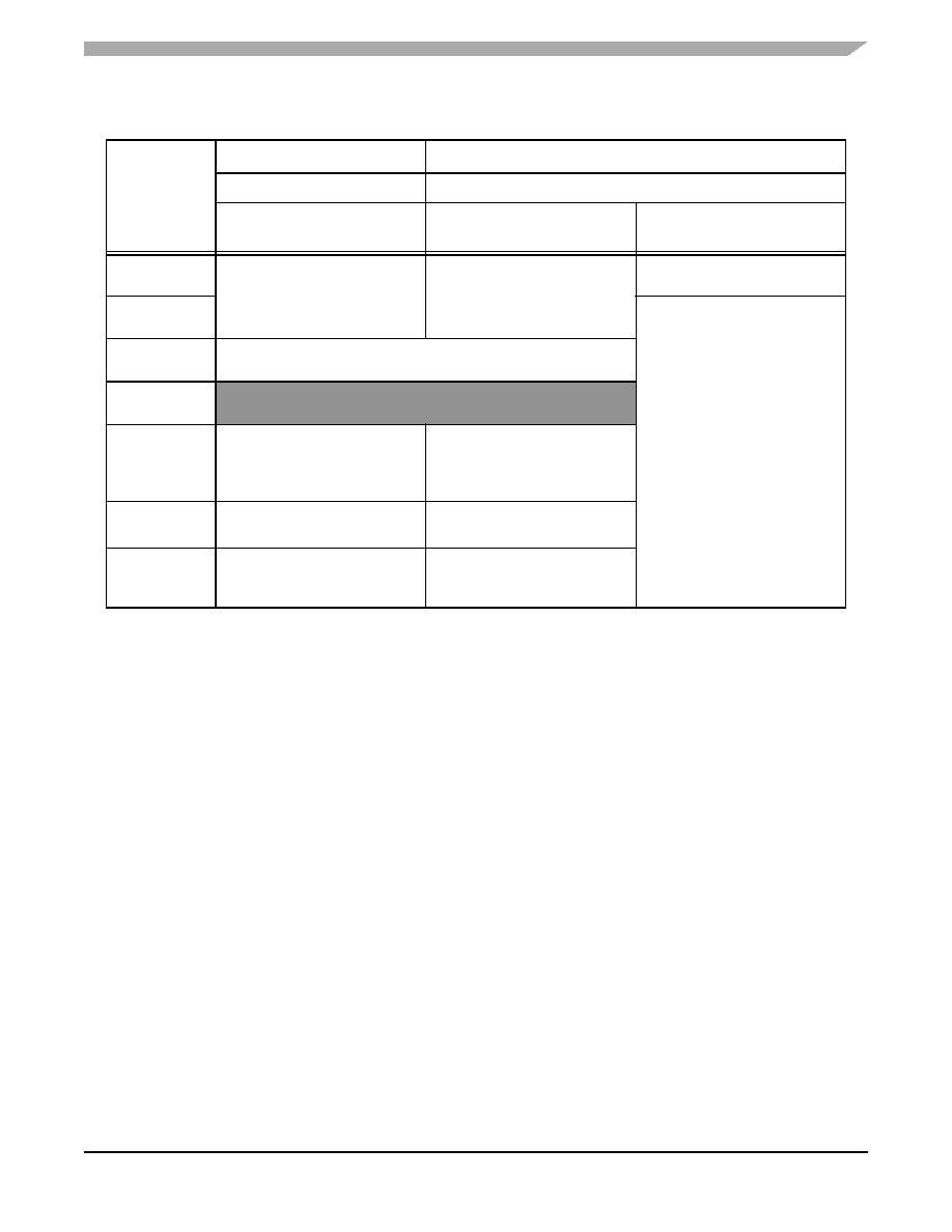
Table 4-4 Program Memory Map at Reset
Begin/End
Address
Mode 0 (MA = 0)
Mode 11 (MA = 1)
1. If Flash Security Mode is enabled, EXTBOOT Mode 1 cannot be used. See Security Features, Part 7.
Internal Boot
External Boot
Internal Boot
16-Bit External Address Bus
EMI_MODE = 02,3
16-Bit External Address Bus
2. This mode provides maximum compatibility with 56F80x parts while operating externally.
3. “EMI_MODE = 0” when EMI_MODE pin is tied to ground at boot up.
EMI_MODE = 14
20-Bit External Address Bus
4. “EMI_MODE = 1” when EMI_MODE pin is tied to VDD at boot up.
P:$1F FFFF
P:$10 0000
External Program Memory5
5. Not accessible in reset configuration, since the address is above P:$00 FFFF. The higher bit address/GPIO (and/or chip
selects) pins must be reconfigured before this external memory is accessible.
External Program Memory5
P:$0F FFFF
P:$03 0000
External Program Memory
COP Reset Address = 02 0002
Boot Location = 02 00006
6. Booting from this external address allows prototyping of the internal Boot Flash.
P:$02 FFFF
P:$02 F800
On-Chip Program RAM
4KB
P:$02 F7FF
P:$02 2000
Reserved
116KB
P:$02 1FFF
P:$02 0000
Boot Flash
16KB
COP Reset Address = 02 0002
Boot Location = 02 0000
Boot Flash
16KB
(Not Used for Boot in this Mode)
P:$01 FFFF
P:$01 0000
Internal Program Flash7
128KB
7. Two independent program Flash blocks allow one to be programmed/erased while executing from another. Each block
must have its own mass erase.
Internal Program Flash
128KB
P:$00 FFFF
P:$00 0000
Internal Program Flash7
128KB
External Program RAM
COP Reset Address = 00 0002
Boot Location = 00 0000
Because
of
an
order
from
the
United
States
International
Trade
Commission,
BGA-packaged
product
lines
and
part
numbers
indicated
here
currently
are
not
available
from
Freescale
for
import
or
sale
in
the
United
States
prior
to
September
2010:
MC56F8357,
MC56F8157
相關PDF資料 |
PDF描述 |
|---|---|
| MC56F8166VFV | 16-BIT, 120 MHz, OTHER DSP, PQFP144 |
| MC56F8366MFVE | 16-BIT, 120 MHz, OTHER DSP, PQFP144 |
| MC56F8366VFVE | 16-BIT, 120 MHz, OTHER DSP, PQFP144 |
| MC56F8366VFV60 | 16-BIT, 120 MHz, OTHER DSP, PQFP144 |
| MC56F8335MFGE | 4-BIT, 120 MHz, OTHER DSP, PQFP128 |
相關代理商/技術參數(shù) |
參數(shù)描述 |
|---|---|
| MC56F8357VPYE | 功能描述:數(shù)字信號處理器和控制器 - DSP, DSC 16 BIT HYBRID CNTRLR RoHS:否 制造商:Microchip Technology 核心:dsPIC 數(shù)據(jù)總線寬度:16 bit 程序存儲器大小:16 KB 數(shù)據(jù) RAM 大小:2 KB 最大時鐘頻率:40 MHz 可編程輸入/輸出端數(shù)量:35 定時器數(shù)量:3 設備每秒兆指令數(shù):50 MIPs 工作電源電壓:3.3 V 最大工作溫度:+ 85 C 封裝 / 箱體:TQFP-44 安裝風格:SMD/SMT |
| MC56F8357VVF | 制造商:FREESCALE 制造商全稱:Freescale Semiconductor, Inc 功能描述:16-bit Digital Signal Controllers |
| MC56F8357VVFE | 功能描述:數(shù)字信號處理器和控制器 - DSP, DSC 16 BIT HYBRID CNTRLR RoHS:否 制造商:Microchip Technology 核心:dsPIC 數(shù)據(jù)總線寬度:16 bit 程序存儲器大小:16 KB 數(shù)據(jù) RAM 大小:2 KB 最大時鐘頻率:40 MHz 可編程輸入/輸出端數(shù)量:35 定時器數(shù)量:3 設備每秒兆指令數(shù):50 MIPs 工作電源電壓:3.3 V 最大工作溫度:+ 85 C 封裝 / 箱體:TQFP-44 安裝風格:SMD/SMT |
| MC56F8357VVFEJ | 制造商:Freescale Semiconductor 功能描述:16 BIT HYBRID CONTROLLER - Bulk |
| MC56F8365 | 制造商:FREESCALE 制造商全稱:Freescale Semiconductor, Inc 功能描述:16-bit Digital Signal Controllers |
發(fā)布緊急采購,3分鐘左右您將得到回復。