- 您現在的位置:買賣IC網 > PDF目錄45220 > MC68HC05F8B (FREESCALE SEMICONDUCTOR INC) 8-BIT, MROM, 1.8 MHz, MICROCONTROLLER, PDIP56 PDF資料下載
參數資料
| 型號: | MC68HC05F8B |
| 廠商: | FREESCALE SEMICONDUCTOR INC |
| 元件分類: | 微控制器/微處理器 |
| 英文描述: | 8-BIT, MROM, 1.8 MHz, MICROCONTROLLER, PDIP56 |
| 封裝: | PLASTIC, SDIP-56 |
| 文件頁數: | 76/126頁 |
| 文件大?。?/td> | 1084K |
| 代理商: | MC68HC05F8B |
第1頁第2頁第3頁第4頁第5頁第6頁第7頁第8頁第9頁第10頁第11頁第12頁第13頁第14頁第15頁第16頁第17頁第18頁第19頁第20頁第21頁第22頁第23頁第24頁第25頁第26頁第27頁第28頁第29頁第30頁第31頁第32頁第33頁第34頁第35頁第36頁第37頁第38頁第39頁第40頁第41頁第42頁第43頁第44頁第45頁第46頁第47頁第48頁第49頁第50頁第51頁第52頁第53頁第54頁第55頁第56頁第57頁第58頁第59頁第60頁第61頁第62頁第63頁第64頁第65頁第66頁第67頁第68頁第69頁第70頁第71頁第72頁第73頁第74頁第75頁當前第76頁第77頁第78頁第79頁第80頁第81頁第82頁第83頁第84頁第85頁第86頁第87頁第88頁第89頁第90頁第91頁第92頁第93頁第94頁第95頁第96頁第97頁第98頁第99頁第100頁第101頁第102頁第103頁第104頁第105頁第106頁第107頁第108頁第109頁第110頁第111頁第112頁第113頁第114頁第115頁第116頁第117頁第118頁第119頁第120頁第121頁第122頁第123頁第124頁第125頁第126頁
MC68HC05F8
MOTOROLA
6-5
TIMERS
6
corresponding input edge bit (IEDG). Reset does not affect the contents of the Input Capture
register.
The result obtained from an input capture will be one greater than the value of the free-running
counter on the rising edge of the internal bus clock preceding the external transition. This delay is
required for internal synchronization. Resolution is zero or one count of the free-running counter,
which is 4xRTB internal bus clock cycles.
The free-running counter contents are transferred to the Input Capture register on each valid
signal transition whether the input capture ag (ICF) is set or clear. The Input Capture register
always contains the free-running counter value that corresponds to the most recent input
capture.After a read of the input capture register MSB ($1A), the counter transfer is inhibited until
the LSB ($1B) is also read. This characteristic causes the time used in the input capture software
routine and its interaction with the main program to determine the minimum pulse period. A read
of the input capture register LSB ($1B) does not inhibit the free-running counter transfer since they
occur on opposite edges of the internal bus clock.
6.1.4
Timer Control Register (TCR)
The TCR is a read/write register containing ve control bits. Three bits control interrupts
associated with the three ag bits found in the timer status register (discussed below). The other
two bits control: 1) which edge is signicant to the input capture edge detector (i.e., negative or
positive), and 2) the next value to be clocked to the Output Level registers in response to a
successful output compare. The Timer Control register and the free-running counter are the only
sections of the timer affected by reset. The TCMP pin is forced low during external reset and stays
low until a valid compare changes them to high. Denition of each bit is as follows:
ICIE - Input Capture Interrupt Enable
1 (set)
–
Input Capture interrupt enabled.
0 (clear) –
Input Capture interrupt disabled.
OCIE - Output Compare Interrupt Enable
1 (set)
–
Output Compare interrupt enabled.
0 (clear) –
Output Compare interrupt disabled.
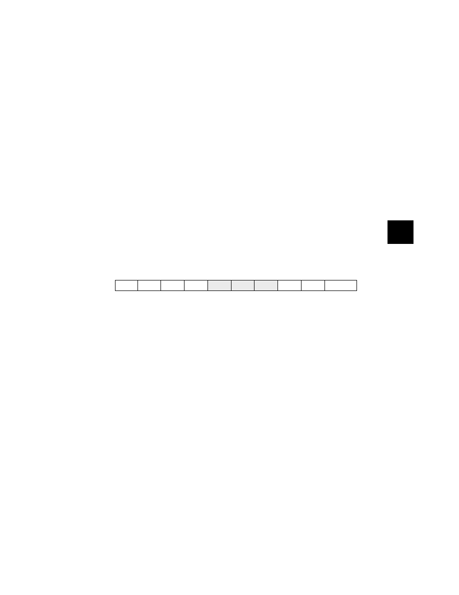
Address
bit 7
bit 6
bit 5
bit 4
bit 3
bit 2
bit 1
bit 0
State
on Reset
$18
ICIE
OCIE
TOIE
0
IEDG
OLVL
0000 00u0
TPG
51
F
re
e
sc
a
le
S
e
m
ic
o
n
d
u
c
to
r,
I
Freescale Semiconductor, Inc.
For More Information On This Product,
Go to: www.freescale.com
n
c
..
.
F
re
e
sc
a
le
S
e
m
ic
o
n
d
u
c
to
r,
In
c
..
.
Freescale Semiconductor, Inc.
For More Information On This Product,
Go to: www.freescale.com
相關PDF資料 |
PDF描述 |
|---|---|
| MC68HC05F8FU | 8-BIT, MROM, 1.8 MHz, MICROCONTROLLER, PQFP64 |
| MC68HC05I8FU | 8-BIT, MROM, 2 MHz, MICROCONTROLLER, PQFP64 |
| MC68HC05J1DW | 8-BIT, MROM, 2.1 MHz, MICROCONTROLLER, PDSO20 |
| MC68HC05J1CP | 8-BIT, MROM, 2.1 MHz, MICROCONTROLLER, PDIP20 |
| MC68HC05J5AJDWR2 | 8-BIT, MROM, 2.1 MHz, MICROCONTROLLER, PDSO16 |
相關代理商/技術參數 |
參數描述 |
|---|---|
| MC68HC05J1 | 制造商:MOTOROLA 制造商全稱:Motorola, Inc 功能描述:HCMOS MICROCONTROLLER UNIT |
| MC68HC05J1A | 制造商:FREESCALE 制造商全稱:Freescale Semiconductor, Inc 功能描述:Microcontrollers |
| MC68HC05J1ACDW | 制造商:FREESCALE 制造商全稱:Freescale Semiconductor, Inc 功能描述:Microcontrollers |
| MC68HC05J1ACP | 制造商:FREESCALE 制造商全稱:Freescale Semiconductor, Inc 功能描述:Microcontrollers |
| MC68HC05J1ADW | 制造商:FREESCALE 制造商全稱:Freescale Semiconductor, Inc 功能描述:Microcontrollers |
發(fā)布緊急采購,3分鐘左右您將得到回復。