- 您現(xiàn)在的位置:買賣IC網(wǎng) > PDF目錄69030 > MC9S08LL16CLF (FREESCALE SEMICONDUCTOR INC) 8-BIT, FLASH, 20 MHz, MICROCONTROLLER, PQFP48 PDF資料下載
參數(shù)資料
| 型號: | MC9S08LL16CLF |
| 廠商: | FREESCALE SEMICONDUCTOR INC |
| 元件分類: | 微控制器/微處理器 |
| 英文描述: | 8-BIT, FLASH, 20 MHz, MICROCONTROLLER, PQFP48 |
| 封裝: | ROHS COMPLIANT, LQFP-48 |
| 文件頁數(shù): | 2/44頁 |
| 文件大小: | 951K |
| 代理商: | MC9S08LL16CLF |
第1頁當前第2頁第3頁第4頁第5頁第6頁第7頁第8頁第9頁第10頁第11頁第12頁第13頁第14頁第15頁第16頁第17頁第18頁第19頁第20頁第21頁第22頁第23頁第24頁第25頁第26頁第27頁第28頁第29頁第30頁第31頁第32頁第33頁第34頁第35頁第36頁第37頁第38頁第39頁第40頁第41頁第42頁第43頁第44頁

MC9S08LL16 Series MCU Data Sheet, Rev. 6
Electrical Characteristics
Freescale Semiconductor
10
NOTE
The classification is shown in the column labeled “C” in the parameter
tables where appropriate.
3.3
Absolute Maximum Ratings
Absolute maximum ratings are stress ratings only, and functional operation at the maxima is not
guaranteed. Stress beyond the limits specified in Table 4 may affect device reliability or cause permanent
damage to the device. For functional operating conditions, refer to the remaining tables in this section.
This device contains circuitry protecting against damage due to high static voltage or electrical fields;
however, it is advised that normal precautions be taken to avoid application of any voltages higher than
maximum-rated voltages to this high-impedance circuit. Reliability of operation is enhanced if unused
inputs are tied to an appropriate logic voltage level (for instance, either VSS or VDD) or the programmable
pull-up resistor associated with the pin is enabled.
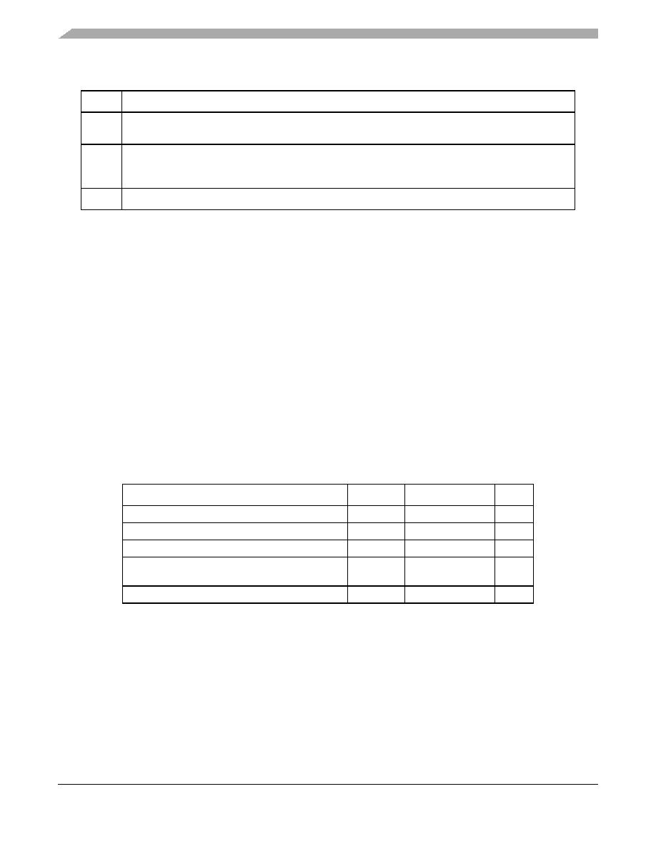
Table 3. Parameter Classifications
P
Those parameters are guaranteed during production testing on each individual device.
C
Those parameters are achieved by the design characterization by measuring a statistically relevant
sample size across process variations.
T
Those parameters are achieved by design characterization on a small sample size from typical devices
under typical conditions unless otherwise noted. All values shown in the typical column are within this
category.
D
Those parameters are derived mainly from simulations.
Table 4. Absolute Maximum Ratings
Rating
Symbol
Value
Unit
Supply voltage
VDD
–0.3 to 3.8
V
Maximum current into VDD
IDD
120
mA
Digital input voltage
VIn
–0.3 to VDD +0.3
V
Instantaneous maximum current
Single pin limit (applies to all port pins)1, 2, 3
1
Input must be current limited to the value specified. To determine the value of the required
current-limiting resistor, calculate resistance values for positive (VDD) and negative (VSS) clamp
voltages, then use the larger of the two resistance values.
2 All functional non-supply pins, except for PTB2 are internally clamped to V
SS and VDD.
3 Power supply must maintain regulation within operating V
DD range during instantaneous and
operating maximum current conditions. If positive injection current (VIn > VDD) is greater than
IDD, the injection current may flow out of VDD and could result in external power supply going
out of regulation. Ensure external VDD load will shunt current greater than maximum injection
current. This will be the greatest risk when the MCU is not consuming power. Examples are: if
no system clock is present, or if the clock rate is very low (which would reduce overall power
consumption).
ID
25
mA
Storage temperature range
Tstg
–55 to 150
C
相關PDF資料 |
PDF描述 |
|---|---|
| MC9S08LL16CGT | 8-BIT, FLASH, 20 MHz, MICROCONTROLLER, QCC48 |
| MC9S08LL64CLK | 8-BIT, FLASH, 40 MHz, MICROCONTROLLER, PQFP80 |
| MC9S08MM128VLH | 8-BIT, FLASH, 48 MHz, MICROCONTROLLER, PQFP64 |
| MC9S08MM128VMB | 8-BIT, FLASH, 48 MHz, MICROCONTROLLER, PBGA81 |
| MC9S08MM32AVLH | 8-BIT, FLASH, 48 MHz, MICROCONTROLLER, PQFP64 |
相關代理商/技術參數(shù) |
參數(shù)描述 |
|---|---|
| MC9S08LL16CLF | 制造商:Freescale Semiconductor 功能描述:IC 8BIT MCU HCS08 20MHZ LQFP-48 |
| MC9S08LL16CLFR | 制造商:Freescale Semiconductor 功能描述:8-BIT HCS08 CISC 16KB FLASH 2.5V/3.3V 48-PIN LQFP T/R - Tape and Reel |
| MC9S08LL16CLH | 功能描述:8位微控制器 -MCU 8BIT 16KFLASH 2KRAM RoHS:否 制造商:Silicon Labs 核心:8051 處理器系列:C8051F39x 數(shù)據(jù)總線寬度:8 bit 最大時鐘頻率:50 MHz 程序存儲器大小:16 KB 數(shù)據(jù) RAM 大小:1 KB 片上 ADC:Yes 工作電源電壓:1.8 V to 3.6 V 工作溫度范圍:- 40 C to + 105 C 封裝 / 箱體:QFN-20 安裝風格:SMD/SMT |
| MC9S08LL36 | 制造商:FREESCALE 制造商全稱:Freescale Semiconductor, Inc 功能描述:Technical Data |
| MC9S08LL36CLH | 功能描述:8位微控制器 -MCU S08 CPU, 36K FLASH, 64LQFP RoHS:否 制造商:Silicon Labs 核心:8051 處理器系列:C8051F39x 數(shù)據(jù)總線寬度:8 bit 最大時鐘頻率:50 MHz 程序存儲器大小:16 KB 數(shù)據(jù) RAM 大小:1 KB 片上 ADC:Yes 工作電源電壓:1.8 V to 3.6 V 工作溫度范圍:- 40 C to + 105 C 封裝 / 箱體:QFN-20 安裝風格:SMD/SMT |
發(fā)布緊急采購,3分鐘左右您將得到回復。