- 您現(xiàn)在的位置:買賣IC網(wǎng) > PDF目錄359153 > MCF52235 (飛思卡爾半導體(中國)有限公司) ColdFire Microcontroller PDF資料下載
參數(shù)資料
| 型號: | MCF52235 |
| 廠商: | 飛思卡爾半導體(中國)有限公司 |
| 英文描述: | ColdFire Microcontroller |
| 中文描述: | ColdFire微控制器 |
| 文件頁數(shù): | 34/50頁 |
| 文件大小: | 656K |
| 代理商: | MCF52235 |
第1頁第2頁第3頁第4頁第5頁第6頁第7頁第8頁第9頁第10頁第11頁第12頁第13頁第14頁第15頁第16頁第17頁第18頁第19頁第20頁第21頁第22頁第23頁第24頁第25頁第26頁第27頁第28頁第29頁第30頁第31頁第32頁第33頁當前第34頁第35頁第36頁第37頁第38頁第39頁第40頁第41頁第42頁第43頁第44頁第45頁第46頁第47頁第48頁第49頁第50頁
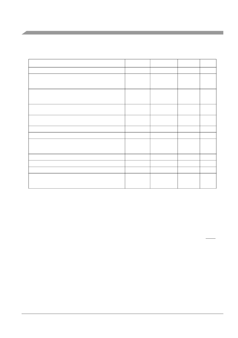
MCF52235 ColdFire Microcontroller, Rev. 3
Preliminary Electrical Characteristics
Freescale Semiconductor
34
Crystal start-up time
5, 6
t
cst
—
10
ms
EXTAL input high voltage
Crystal reference
External reference
V
IHEXT
V
DD
- 1.0
2.0
V
DD
V
DD
V
EXTAL input low voltage
Crystal reference
External reference
V
ILEXT
V
SS
V
SS
1.0
0.8
V
XTAL output high voltage
I
OH
= 1.0 mA
XTAL output low voltage
I
OL
= 1.0 mA
XTAL load capacitance
7
PLL lock time
5,9
Power-up to lock time
5, 7,8
With crystal reference
Without crystal reference
Duty cycle of reference
5
V
OL
V
DD
–1.0
—
V
V
OL
—
0.5
V
—
—
pF
t
lpll
t
lplk
—
500
μ
s
—
—
10.5
500
ms
μ
s
t
dc
f
UL
fLCK
40
60
% f
sys
% f
sys
% f
sys
Frequency un-LOCK range
–1.5
1.5
Frequency LOCK range
CLKOUT period Jitter
5, 6, 8, 9,10
, measured at f
SYS
Max
Peak-to-peak jitter (clock edge to clock edge)
Long term jitter (averaged over 2 ms interval)
–0.75
0.75
C
jitter
—
—
10
.01
% f
sys
1
Input to the PLL is limited to 10 MHz max; however, the PLL divider can accept up to 40 MHz. The input must be
divided down to a frequency no greater than 10 MHz. This is controlled by register CCHR.
2
All internal registers retain data at 0 Hz.
3
Loss of reference frequency is the reference frequency detected internally that transitions the PLL into self-clocked
mode.
4
Self-clocked mode frequency is the frequency that the PLL operates at when the reference frequency falls below f
LOR
with default MFD/RFD settings.
5
This parameter is characterized before qualification rather than 100% tested.
6
Proper PC board layout procedures must be followed to achieve specifications.
7
Load capacitance determined from crystal manufacturer specifications and include circuit board parasitics.
8
Assuming a reference is available at power up, lock time is measured from the time V
DD
and V
DDPLL
are valid to RSTO
negating. If the crystal oscillator is the reference for the PLL, the crystal start up time must be added to the PLL lock
time to determine the total start-up time.
9
Jitter is the average deviation from the programmed frequency measured over the specified interval at maximum f
sys
.
Measurements are made with the device powered by filtered supplies and clocked by a stable external clock signal.
Noise injected into the PLL circuitry via V
DDPLL
and V
SSPLL
and variation in crystal oscillator frequency increase the
C
jitter
percentage for a given interval
10
Based on slow system clock of 40 MHz measured at f
sys
max.
Table 25. PLL Electrical Specifications (continued)
(V
DD
and V
DDPLL
= 2.7 to 3.6 V, V
SS
= V
SSPLL
= 0 V)
Characteristic
Symbol
Min
Max
Unit
相關PDF資料 |
PDF描述 |
|---|---|
| MCF5232CAB80 | Integrated Microprocessor Hardware Specification |
| MCF5232 | Integrated Microprocessor Hardware Specification |
| MCF5249 | CodeWarrior Development Studio for ColdFire㈢ Architectures |
| MCF5251_07 | ColdFire㈢ Microprocessor Data Sheet |
| MCF5251 | ColdFire Processor |
相關代理商/技術參數(shù) |
參數(shù)描述 |
|---|---|
| MCF52235_06 | 制造商:FREESCALE 制造商全稱:Freescale Semiconductor, Inc 功能描述:ColdFire㈢ Microcontroller |
| MCF52235_07 | 制造商:FREESCALE 制造商全稱:Freescale Semiconductor, Inc 功能描述:Microcontroller |
| MCF52235_10 | 制造商:FREESCALE 制造商全稱:Freescale Semiconductor, Inc 功能描述:MCF52235 ColdFire Microcontroller Data Sheet |
| MCF52235CAL60 | 功能描述:32位微控制器 - MCU KIRIN2E EPP RoHS:否 制造商:Texas Instruments 核心:C28x 處理器系列:TMS320F28x 數(shù)據(jù)總線寬度:32 bit 最大時鐘頻率:90 MHz 程序存儲器大小:64 KB 數(shù)據(jù) RAM 大小:26 KB 片上 ADC:Yes 工作電源電壓:2.97 V to 3.63 V 工作溫度范圍:- 40 C to + 105 C 封裝 / 箱體:LQFP-80 安裝風格:SMD/SMT |
| MCF52235CAL60A | 制造商:Freescale Semiconductor 功能描述:KIRIN2E EPP - REV A - Bulk |
發(fā)布緊急采購,3分鐘左右您將得到回復。