- 您現(xiàn)在的位置:買賣IC網(wǎng) > PDF目錄359168 > MK41T56S00TR (意法半導(dǎo)體) 512 bit 64b x8 Serial Access TIMEKEEPER SRAM PDF資料下載
參數(shù)資料
| 型號(hào): | MK41T56S00TR |
| 廠商: | 意法半導(dǎo)體 |
| 英文描述: | 512 bit 64b x8 Serial Access TIMEKEEPER SRAM |
| 中文描述: | 512位64B條x8串行SRAM的訪問計(jì)時(shí)器 |
| 文件頁數(shù): | 5/15頁 |
| 文件大小: | 102K |
| 代理商: | MK41T56S00TR |
Symbol
Parameter
Min
Max
Unit
t
PD
SCL and SDA at V
IH
before Power Down
0
ns
t
FB
V
PFD
(min) to V
SO
V
CC
Fall Time
300
μ
s
t
RB
V
SO
to V
PFD
(min) V
CC
Rise Time
100
μ
s
t
REC
SCL and SDA at V
IH
after Power Up
200
μ
s
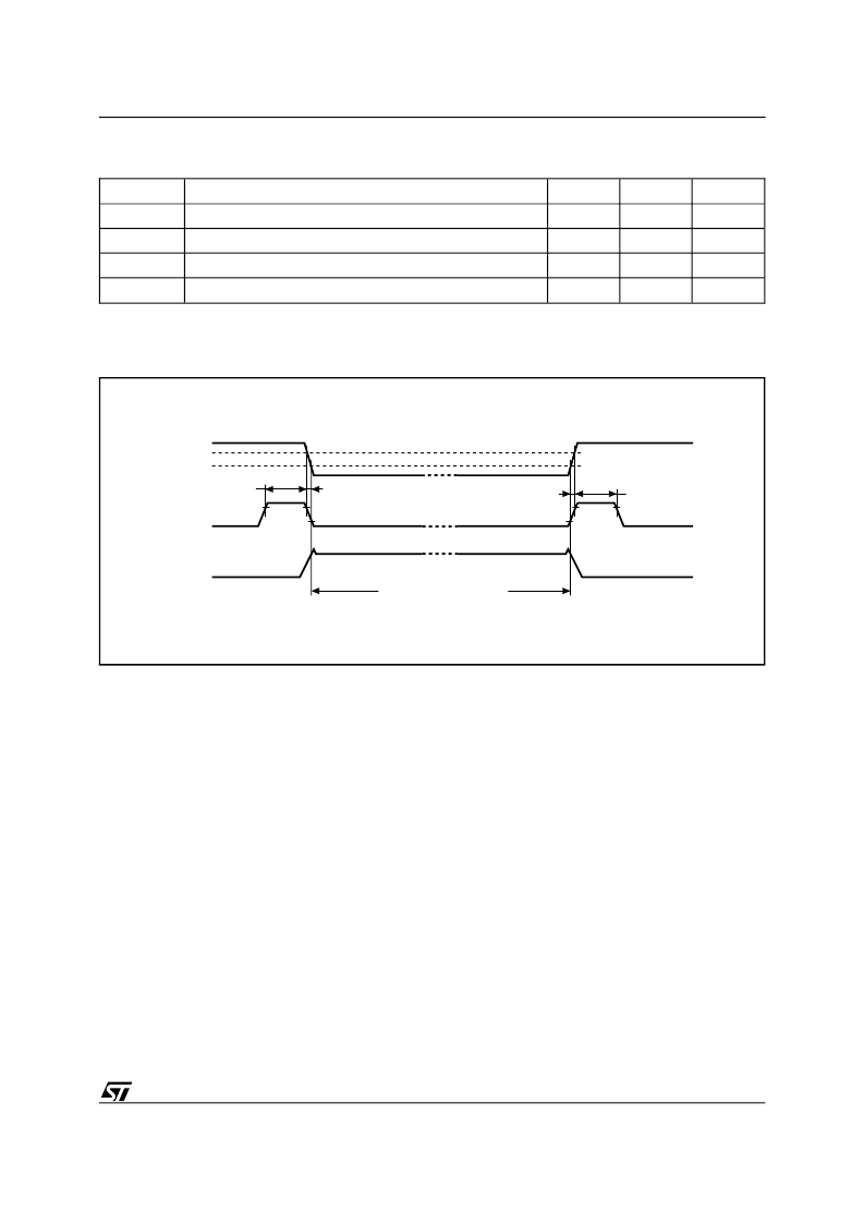
Table 9. Power Down/Up Mode AC Characteristics
(T
A
= 0 to 70
°
C or –40 to 85
°
C)
AI00595
VCC
VPFD
VSO
tFB
tREC
tPD
tRB
DATA RETENTION TIME
SDA
SCL
IBAT
Figure 5. Power Down/Up Mode AC Waveforms
OPERATION
(cont’d)
The clock continually monitors V
CC
for an out of
tolerance condition. Should V
CC
fall below V
PFD
,
the device terminates an access in progress and
resets the device address counter. Inputs to the
device will not be recognized at this time to prevent
erroneous data from being written to the device
from an out of tolerance system. When V
CC
falls
below V
BAT
, the device automatically switches over
to the battery and powers down into an ultra low
current mode of operation to conserve battery life.
Upon power-up, the device switches from battery
to V
CC
at V
BAT
and recognizes inputs when V
CC
goes above V
PFD
volts.
2-WIRE BUS CHARACTERISTICS
This bus is intended for communication between
different ICs. It consists of two lines: one bi-direc-
tional for data signals (SDA) and one for clock
signals (SCL). Both the SDA and the SCL lines
must be connected to a positive supply voltage via
a pull-up resistor.
The following protocol has been defined:
– Data transfer may be initiated only when the
bus is not busy.
– During data transfer, the data line must remain
stable whenever the clock line is High.
– Changes in the data line while the clock line is
High will be interpreted as control signals.
5/15
MK41T56, MKI41T56
相關(guān)PDF資料 |
PDF描述 |
|---|---|
| MK41T56S00 | 512 bit 64b x8 Serial Access TIMEKEEPER SRAM |
| MK45H03K | VERY FAST CMOS 512/1K/2K x9BiPORT FIFO |
| MK45H03N | VERY FAST CMOS 512/1K/2K x9BiPORT FIFO |
| MK45H03 | VERY FAST CMOS 512/1K/2K x9BiPORT FIFO |
| MK48Z02 | FILTER SAW BNDPASS 43.75MHZ 5SIP |
相關(guān)代理商/技術(shù)參數(shù) |
參數(shù)描述 |
|---|---|
| MK4200 | 制造商:Abus 功能描述:Bulk |
| MK4222F | 制造商:Ohmite Mfg Co 功能描述: |
| MK424BS | 制造商:POP 功能描述: |
| MK4321F | 制造商:Ohmite Mfg Co 功能描述:Res Metal Film 4.32K Ohm 1% 1/4W ±50ppm/°C Conformal AXL Thru-Hole Ammo Pack |
| MK43A232-008 | 制造商:TE Connectivity 功能描述: |
發(fā)布緊急采購,3分鐘左右您將得到回復(fù)。