- 您現(xiàn)在的位置:買賣IC網 > PDF目錄369919 > MMC2001 (MOTOROLA INC) Highly Integrated, Low-Power, 32-Bit Microcontroller PDF資料下載
參數(shù)資料
| 型號: | MMC2001 |
| 廠商: | MOTOROLA INC |
| 元件分類: | 微控制器/微處理器 |
| 英文描述: | Highly Integrated, Low-Power, 32-Bit Microcontroller |
| 中文描述: | 32-BIT, 34 MHz, RISC PROCESSOR, PQFP144 |
| 封裝: | PLASTIC, TQFP-144 |
| 文件頁數(shù): | 34/260頁 |
| 文件大小: | 3848K |
| 代理商: | MMC2001 |
第1頁第2頁第3頁第4頁第5頁第6頁第7頁第8頁第9頁第10頁第11頁第12頁第13頁第14頁第15頁第16頁第17頁第18頁第19頁第20頁第21頁第22頁第23頁第24頁第25頁第26頁第27頁第28頁第29頁第30頁第31頁第32頁第33頁當前第34頁第35頁第36頁第37頁第38頁第39頁第40頁第41頁第42頁第43頁第44頁第45頁第46頁第47頁第48頁第49頁第50頁第51頁第52頁第53頁第54頁第55頁第56頁第57頁第58頁第59頁第60頁第61頁第62頁第63頁第64頁第65頁第66頁第67頁第68頁第69頁第70頁第71頁第72頁第73頁第74頁第75頁第76頁第77頁第78頁第79頁第80頁第81頁第82頁第83頁第84頁第85頁第86頁第87頁第88頁第89頁第90頁第91頁第92頁第93頁第94頁第95頁第96頁第97頁第98頁第99頁第100頁第101頁第102頁第103頁第104頁第105頁第106頁第107頁第108頁第109頁第110頁第111頁第112頁第113頁第114頁第115頁第116頁第117頁第118頁第119頁第120頁第121頁第122頁第123頁第124頁第125頁第126頁第127頁第128頁第129頁第130頁第131頁第132頁第133頁第134頁第135頁第136頁第137頁第138頁第139頁第140頁第141頁第142頁第143頁第144頁第145頁第146頁第147頁第148頁第149頁第150頁第151頁第152頁第153頁第154頁第155頁第156頁第157頁第158頁第159頁第160頁第161頁第162頁第163頁第164頁第165頁第166頁第167頁第168頁第169頁第170頁第171頁第172頁第173頁第174頁第175頁第176頁第177頁第178頁第179頁第180頁第181頁第182頁第183頁第184頁第185頁第186頁第187頁第188頁第189頁第190頁第191頁第192頁第193頁第194頁第195頁第196頁第197頁第198頁第199頁第200頁第201頁第202頁第203頁第204頁第205頁第206頁第207頁第208頁第209頁第210頁第211頁第212頁第213頁第214頁第215頁第216頁第217頁第218頁第219頁第220頁第221頁第222頁第223頁第224頁第225頁第226頁第227頁第228頁第229頁第230頁第231頁第232頁第233頁第234頁第235頁第236頁第237頁第238頁第239頁第240頁第241頁第242頁第243頁第244頁第245頁第246頁第247頁第248頁第249頁第250頁第251頁第252頁第253頁第254頁第255頁第256頁第257頁第258頁第259頁第260頁
MOTOROLA
2-12
INTEGER CPU
MMC2001
REFERENCE MANUAL
The MCORE receives a clock input (CLK) from an external clock source and gener-
ates two internal clocks (C1 and C2). The CLK input sets the frequency of operation
for the bus interface directly. The clock source monitors the MCORE low power
mode outputs (LPMD[1:0]) and controls the clock input to the MCORE accordingly
by forcing the clocks low for low-power operation.
Data transfers occur between an internal register and the external bus. The internal
register connects to the external data bus through the internal data bus and a data
multiplexer. The data multiplexer establishes the necessary connections for different
combinations of address and data sizes. This multiplexer is physically positioned in
the overall system to minimize power consumption by minimizing loading and reduc-
ing unnecessary signal transitions. Logically, however, it is considered part of the
MCORE.
The MCORE does not support dynamic bus sizing and expects the referenced
device to accept the requested access width. Peripherals with an interface width of N
bits should not define internal registers greater than N bits wide.
Misaligned transfers are not supported. The MCORE interface may drive the
ADDR[1:0] address lines to a value which is not representative of an aligned transfer,
but expects aligned data to be transferred. ADDR[1:0] should be selectively ignored
by external logic, depending on the size of the transfer.
The data multiplexer takes the four bytes of the core interface data bus and routes
them to their required positions to interface properly to memory or peripherals. The
external multiplexer connections to memory are controlled on a byte granularity and
are referred to as MB0–MB3, where MB0 resides at byte address 0 (mod 4) and MB3
resides at byte address 3 (mod 4). For example, MB0 would normally be routed to
DATA[31:24] on a word transfer, but it can also be routed to DATA[7:0] for supporting
a byte data transfer. The same is true for any of the other operand bytes.
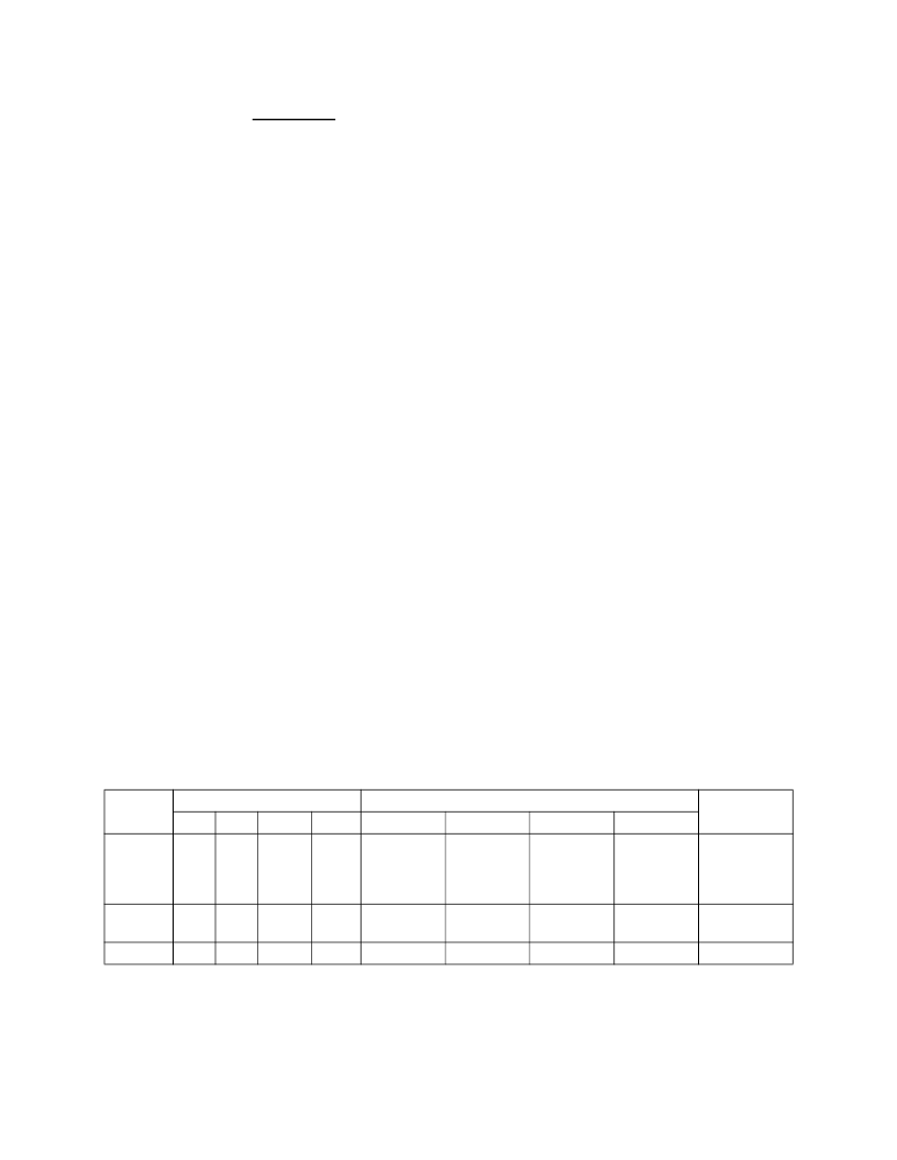
Figure 2-6
shows the connection requirements for the multiplexer. The transfer size
(TSIZ[1:0]) and byte offset (ADDR1 and ADDR0) signals determine the positioning of
the bytes (see
Table 2-3
).
7DEOH,QWHUIDFH5HTXLUHPHQWVIRU5HDGDQG:ULWH&\FOHV
Transfer
Size
Active Interface Bus Sections
Mux
Connections
TSIZ1 TSIZ0 ADDR1 ADDR0 DATA[31:24] DATA[23:16] DATA[15:8]
0
0
0
0
1
1
1
1
1
0
1
X
0
0
X
X
MB0
DATA[7:0]
MB0
MB1
MB2
MB3
MB1
MB3
MB3
Byte
1
1
1
0
0
1
0
1
0
—
—
—
—
—
—
—
—
—
—
—
—
—
—
—
—
a
b
c
d
e
f
g
Halfword
0
0
X
MB0
MB2
MB2
Word
MB1
相關PDF資料 |
PDF描述 |
|---|---|
| MMC2075 | Integrated Processor with Roaming FLEX Decoder |
| MMC2075VF001 | Integrated Processor with Roaming FLEX Decoder |
| MMC2080 | Integrated Processor with Roaming FLEX Decoder |
| MMC2080VF001 | Integrated Processor with Roaming FLEX Decoder |
| MMC2107 | HCMOS Microcontroller Unit |
相關代理商/技術參數(shù) |
參數(shù)描述 |
|---|---|
| MMC2001DDRM | 制造商:未知廠家 制造商全稱:未知廠家 功能描述:M-CORE MMC2001 Device Driver Reference Manual |
| MMC2001HCAB33B | 功能描述:32位微控制器 - MCU PBFREE MMC2001 RoHS:否 制造商:Texas Instruments 核心:C28x 處理器系列:TMS320F28x 數(shù)據總線寬度:32 bit 最大時鐘頻率:90 MHz 程序存儲器大小:64 KB 數(shù)據 RAM 大小:26 KB 片上 ADC:Yes 工作電源電壓:2.97 V to 3.63 V 工作溫度范圍:- 40 C to + 105 C 封裝 / 箱體:LQFP-80 安裝風格:SMD/SMT |
| MMC2075 | 制造商:MOTOROLA 制造商全稱:Motorola, Inc 功能描述:Integrated Processor with Roaming FLEX Decoder |
| MMC2075VF001 | 制造商:MOTOROLA 制造商全稱:Motorola, Inc 功能描述:Integrated Processor with Roaming FLEX Decoder |
| MMC2080 | 制造商:MOTOROLA 制造商全稱:Motorola, Inc 功能描述:Integrated Processor with Roaming FLEX Decoder |
發(fā)布緊急采購,3分鐘左右您將得到回復。