- 您現(xiàn)在的位置:買賣IC網 > PDF目錄369923 > MPC107 (Motorola, Inc.) 32-Bit Microprocessor(32位微處理器) PDF資料下載
參數(shù)資料
| 型號: | MPC107 |
| 廠商: | Motorola, Inc. |
| 英文描述: | 32-Bit Microprocessor(32位微處理器) |
| 中文描述: | 32位微處理器(32位微處理器) |
| 文件頁數(shù): | 19/46頁 |
| 文件大小: | 585K |
| 代理商: | MPC107 |
第1頁第2頁第3頁第4頁第5頁第6頁第7頁第8頁第9頁第10頁第11頁第12頁第13頁第14頁第15頁第16頁第17頁第18頁當前第19頁第20頁第21頁第22頁第23頁第24頁第25頁第26頁第27頁第28頁第29頁第30頁第31頁第32頁第33頁第34頁第35頁第36頁第37頁第38頁第39頁第40頁第41頁第42頁第43頁第44頁第45頁第46頁
MPC107 Hardware Specifications (Rev 0.2)
PRELIMINARYSUBJECT TO CHANGE WITHOUT NOTICE
19
Electrical and Thermal Characteristics
1.4.3.3 Output AC Timing SpeciTcation
Table 10 provides the processor bus AC timing speciTcations for the MPC107. See Figure 7 and Figure 8.
Notes:
1
All memory and related interface output signal speciTcations are speciTed from the V
= 1.4 V of the rising edge
of the memory bus clock, SDRAM_SYNC_IN to the TTL level (0.8 or 2.0 V) of the signal in question.
SDRAM_SYNC_IN is the same as PCI_SYNC_IN in 1:1 mode, but is twice the frequency in 2:1 mode (proces-
sor/memory bus clock rising edges occur on every rising and falling edge of PCI_SYNC_IN). See Figure 7.
All PCI signals are measured from OVdd/2 of the rising edge of PCI_SYNC_IN to 0.285*OVdd or 0.615*OVdd of
the signal in question for 3.3 V PCI signaling levels. See Figure 8.
All output timings assume a purely resistive 50 ohm load (See Figure 10). Output timings are measured at the
pin; time-of-ight delays must be added for trace lengths, vias, and connectors in the system.
PCI Bussed signals are composed of the following signals: LOCK, IRDY, C/BE[0D3], PAR, TRDY, FRAME, STOP,
DEVSEL, PERR, SERR, AD[0D31], REQ[4D0], GNT[4D0], IDSEL, INTA.
PCI hold times can be varied, see 1.4.3.3.1 òPCI Signal Output Hold Timingó section for information on program-
mable PCI output hold times. The values shown for item 13a are for PCI compliance.
These speciTcations are for the default driver strengths indicated in Table 4.
2
3
4
5
6
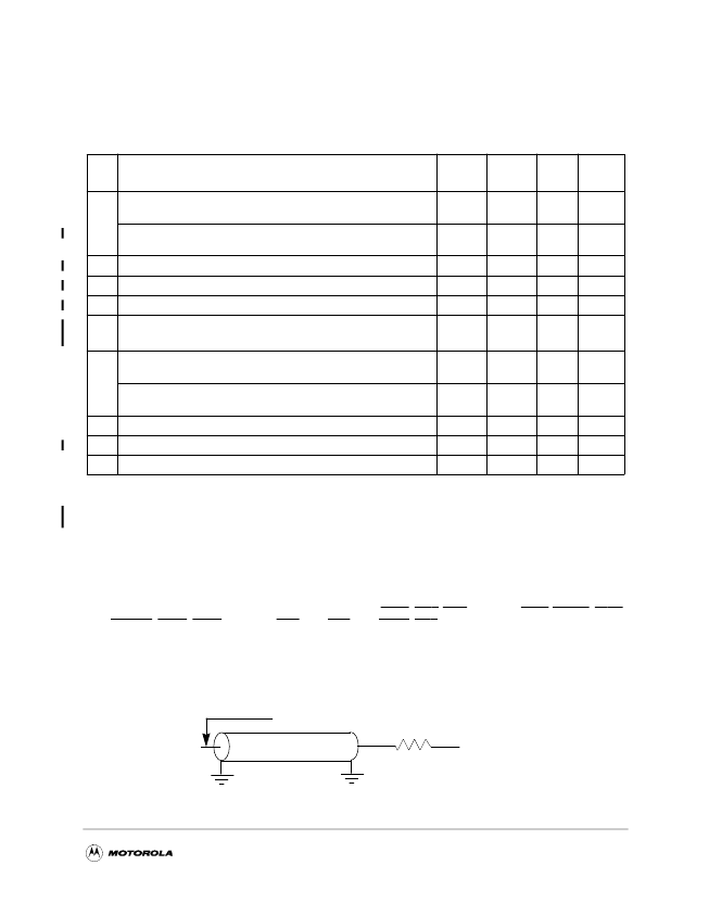
Figure 10 shows the AC Test Load for the MPC107.
Figure 10. AC Test Load for the MPC107
Table 10. Output AC Timing Specifications
At recommended operating conditions (See Table 2) with GVdd = 3.3 V ± 5% and LVdd = 3.3 V ± 5%
Nu
m
Characteristic
3,6
Min
Max
Units
Notes
12a
PCI_SYNC_IN to Output Valid, 66 MHz PCI, with SDMA4 pulled-
down to logic 0 state. See Figure 11.
6.0
ns
2,4
PCI_SYNC_IN to Output Valid, 33 MHz PCI, with SDMA4 in the
default logic 1 state. See Figure 11.
11.0
ns
2,4
12b
Memory Interface Signals, SDRAM_SYNC_IN to Output Valid
5.5
ns
1
12c
Epic, Misc. Debug Signals, SDRAM_SYNC_IN to Output Valid
9.0
ns
1
12d
I
2
C, SDRAM_SYNC_IN to Output Valid
5.0
ns
1
12e
60x Processor Interface Signals
SDRAM_SYNC_IN to Output Valid
5.5
ns
1
13a
Output Hold, 66 MHz PCI, with SDMA4 and SDMA3 pulled-down to
logic 0 states. See Table 11.
1.0
ns
2,4,5
Output Hold, 33 MHz PCI, with SDMA4 in the default logic 1 state
and SDMA3 pulled-down to logic 0 state. See Table 11.
2.0
ns
2,4,5
13b
Output Hold (For All Others)
1
ns
1
14a
PCI_SYNC_IN to Output High Impedance (T
off
for PCI)
14.0
ns
2,4
14b
SDRAM_SYNC_IN to Output High Impedance (For All Others)
TBD
ns
1
OUTPUT
Z
0
= 50
W
OVdd/2
R
L
= 50
W
PIN
Output measurements are made at the device pin.
相關PDF資料 |
PDF描述 |
|---|---|
| MPC505 | Highly Integrated, Low-Power, 32-Bit Microcontroller |
| MPC509 | Highly Integrated, Low-Power, 32-Bit Microcontroller |
| MPC5200BV400 | MPC5200 Hardware Specifications |
| MPC5200CBV266 | MPC5200 Hardware Specifications |
| MPC5200CBV400 | MPC5200 Hardware Specifications |
相關代理商/技術參數(shù) |
參數(shù)描述 |
|---|---|
| MPC-108 | 制造商:Greenlee Textron Inc 功能描述:Unspecified Tools & Accessories ADAPTER,MATING BULKHEAD |
| MPC108100J | 功能描述:厚膜電阻器 - 透孔 MPC10 10R 5% RoHS:否 制造商:Caddock 電阻:27 kOhms 容差:1 % 功率額定值:8 W 溫度系數(shù):50 PPM / C 系列:MS 端接類型:Axial 電壓額定值:2 kV 工作溫度范圍:- 15 C to + 275 C 尺寸:8.89 mm Dia. x 23.11 mm L 封裝:Bulk |
| MPC108101J | 制造商:TE Connectivity 功能描述:RESISTOR 10 WATT 100R 5% |
| MPC108102J | 功能描述:厚膜電阻器 - 透孔 MPC10 1K0 5% RoHS:否 制造商:Caddock 電阻:27 kOhms 容差:1 % 功率額定值:8 W 溫度系數(shù):50 PPM / C 系列:MS 端接類型:Axial 電壓額定值:2 kV 工作溫度范圍:- 15 C to + 275 C 尺寸:8.89 mm Dia. x 23.11 mm L 封裝:Bulk |
| MPC108103J | 功能描述:厚膜電阻器 - 透孔 MPC10 10K 5% RoHS:否 制造商:Caddock 電阻:27 kOhms 容差:1 % 功率額定值:8 W 溫度系數(shù):50 PPM / C 系列:MS 端接類型:Axial 電壓額定值:2 kV 工作溫度范圍:- 15 C to + 275 C 尺寸:8.89 mm Dia. x 23.11 mm L 封裝:Bulk |
發(fā)布緊急采購,3分鐘左右您將得到回復。