- 您現(xiàn)在的位置:買賣IC網(wǎng) > PDF目錄369923 > MPC107 (Motorola, Inc.) 32-Bit Microprocessor(32位微處理器) PDF資料下載
參數(shù)資料
| 型號(hào): | MPC107 |
| 廠商: | Motorola, Inc. |
| 英文描述: | 32-Bit Microprocessor(32位微處理器) |
| 中文描述: | 32位微處理器(32位微處理器) |
| 文件頁(yè)數(shù): | 39/46頁(yè) |
| 文件大小: | 585K |
| 代理商: | MPC107 |
第1頁(yè)第2頁(yè)第3頁(yè)第4頁(yè)第5頁(yè)第6頁(yè)第7頁(yè)第8頁(yè)第9頁(yè)第10頁(yè)第11頁(yè)第12頁(yè)第13頁(yè)第14頁(yè)第15頁(yè)第16頁(yè)第17頁(yè)第18頁(yè)第19頁(yè)第20頁(yè)第21頁(yè)第22頁(yè)第23頁(yè)第24頁(yè)第25頁(yè)第26頁(yè)第27頁(yè)第28頁(yè)第29頁(yè)第30頁(yè)第31頁(yè)第32頁(yè)第33頁(yè)第34頁(yè)第35頁(yè)第36頁(yè)第37頁(yè)第38頁(yè)當(dāng)前第39頁(yè)第40頁(yè)第41頁(yè)第42頁(yè)第43頁(yè)第44頁(yè)第45頁(yè)第46頁(yè)
MPC107 Hardware Specifications (Rev 0.2)
PRELIMINARYSUBJECT TO CHANGE WITHOUT NOTICE
39
System Design Information
1.7 System Design Information
This section provides electrical and thermal design recommendations for successful application of the
MPC107.
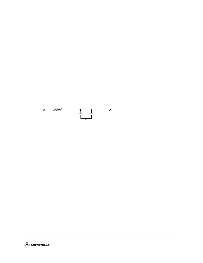
1.7.1 PLL Power Supply Filtering
The AVdd and LAVdd power signals are provided on the MPC107 to provide power to the peripheral logic/
memory bus PLL, the 603e processor PLL, and the SDRAM clock delay-locked loop (DLL), respectively.
To ensure stability of the internal clocks, the power supplied to the AVdd and LAVdd input signals should
be Tltered of any noise in the 500kHz to 10MHz resonant frequency range of the PLLs. A separate circuit
similar to the one shown in Figure 23 using surface mount capacitors with minimum effective series
inductance (ESL) is recommended for each of the AVdd and LAVdd power signal pins. Consistent with the
recommendations of Dr. Howard Johnson in
High Speed Digital Design: A Handbook of Black Magic
(Prentice Hall, 1993), multiple small capacitors of equal value are recommended over using multiple values.
The circuits should be placed as close as possible to the respective input signal pins to minimize noise
coupled from nearby circuits. Routing directly as possible from the capacitors to the input signal pins with
minimal inductance of vias is important but proportionately less critical for the LAVdd pin.
Figure 23. PLL Power Supply Filter Circuit
1.7.2 Power Supply Voltage Sequencing
The notes in Table 2 contain cautions illustrated in Figure 2 about the sequencing of the external bus
voltages and internal voltages of the MPC107. These cautions are necessary for the long term reliability of
the part. If they are violated, the electrostatic discharge (ESD) protection diodes will be forward biased and
excessive current can ow through these diodes. Figure 2 shows a typical ramping voltage sequence where
the DC power sources (voltage regulators and/or power supplies) are connected as shown in Figure 24. The
voltage regulator delay shown in Figure 2 can be zero if the various DC voltage levels are all applied to the
target board at the same time. The ramping voltage sequence shows a scenario in which the Vdd/AVdd/
LAVdd power plane is not loaded as much as the OVdd/GVdd power plane and thus Vdd/AVdd/LAVdd
ramps at a faster rate than OVdd/GVdd.
If the system power supply design does not control the voltage sequencing, the circuit of Figure 24 can be
added to meet these requirements. The MUR420 diodes of Figure 24 control the maximum potential
difference between the 3.3V bus and internal voltages on power-up and the 1N5820 Schottky diodes
regulate the maximum potential difference on power-down.
Vdd
AVdd or LAVdd
10
W
2.2 μF
2.2 μF
GND
Low ESL surface mount capacitors
相關(guān)PDF資料 |
PDF描述 |
|---|---|
| MPC505 | Highly Integrated, Low-Power, 32-Bit Microcontroller |
| MPC509 | Highly Integrated, Low-Power, 32-Bit Microcontroller |
| MPC5200BV400 | MPC5200 Hardware Specifications |
| MPC5200CBV266 | MPC5200 Hardware Specifications |
| MPC5200CBV400 | MPC5200 Hardware Specifications |
相關(guān)代理商/技術(shù)參數(shù) |
參數(shù)描述 |
|---|---|
| MPC-108 | 制造商:Greenlee Textron Inc 功能描述:Unspecified Tools & Accessories ADAPTER,MATING BULKHEAD |
| MPC108100J | 功能描述:厚膜電阻器 - 透孔 MPC10 10R 5% RoHS:否 制造商:Caddock 電阻:27 kOhms 容差:1 % 功率額定值:8 W 溫度系數(shù):50 PPM / C 系列:MS 端接類型:Axial 電壓額定值:2 kV 工作溫度范圍:- 15 C to + 275 C 尺寸:8.89 mm Dia. x 23.11 mm L 封裝:Bulk |
| MPC108101J | 制造商:TE Connectivity 功能描述:RESISTOR 10 WATT 100R 5% |
| MPC108102J | 功能描述:厚膜電阻器 - 透孔 MPC10 1K0 5% RoHS:否 制造商:Caddock 電阻:27 kOhms 容差:1 % 功率額定值:8 W 溫度系數(shù):50 PPM / C 系列:MS 端接類型:Axial 電壓額定值:2 kV 工作溫度范圍:- 15 C to + 275 C 尺寸:8.89 mm Dia. x 23.11 mm L 封裝:Bulk |
| MPC108103J | 功能描述:厚膜電阻器 - 透孔 MPC10 10K 5% RoHS:否 制造商:Caddock 電阻:27 kOhms 容差:1 % 功率額定值:8 W 溫度系數(shù):50 PPM / C 系列:MS 端接類型:Axial 電壓額定值:2 kV 工作溫度范圍:- 15 C to + 275 C 尺寸:8.89 mm Dia. x 23.11 mm L 封裝:Bulk |
發(fā)布緊急采購(gòu),3分鐘左右您將得到回復(fù)。