- 您現(xiàn)在的位置:買賣IC網(wǎng) > PDF目錄45360 > MPC8314EVRAGDA (FREESCALE SEMICONDUCTOR INC) MICROPROCESSOR, PBGA620 PDF資料下載
參數(shù)資料
| 型號: | MPC8314EVRAGDA |
| 廠商: | FREESCALE SEMICONDUCTOR INC |
| 元件分類: | 微控制器/微處理器 |
| 英文描述: | MICROPROCESSOR, PBGA620 |
| 封裝: | 29 X 29 MM, LEAD FREE, PLASTIC, TEPBGA-620 |
| 文件頁數(shù): | 39/106頁 |
| 文件大小: | 1253K |
| 代理商: | MPC8314EVRAGDA |
第1頁第2頁第3頁第4頁第5頁第6頁第7頁第8頁第9頁第10頁第11頁第12頁第13頁第14頁第15頁第16頁第17頁第18頁第19頁第20頁第21頁第22頁第23頁第24頁第25頁第26頁第27頁第28頁第29頁第30頁第31頁第32頁第33頁第34頁第35頁第36頁第37頁第38頁當(dāng)前第39頁第40頁第41頁第42頁第43頁第44頁第45頁第46頁第47頁第48頁第49頁第50頁第51頁第52頁第53頁第54頁第55頁第56頁第57頁第58頁第59頁第60頁第61頁第62頁第63頁第64頁第65頁第66頁第67頁第68頁第69頁第70頁第71頁第72頁第73頁第74頁第75頁第76頁第77頁第78頁第79頁第80頁第81頁第82頁第83頁第84頁第85頁第86頁第87頁第88頁第89頁第90頁第91頁第92頁第93頁第94頁第95頁第96頁第97頁第98頁第99頁第100頁第101頁第102頁第103頁第104頁第105頁第106頁
MPC8314E PowerQUICC II Pro Processor Hardware Specifications, Rev. 0
38
Freescale Semiconductor
USB
10.1.1
USB DC Electrical Characteristics
Table 39 lists the DC electrical characteristics for the USB interface.
10.1.2
USB AC Electrical Specifications
Table 40 lists the general timing parameters of the USB-ULPI interface.
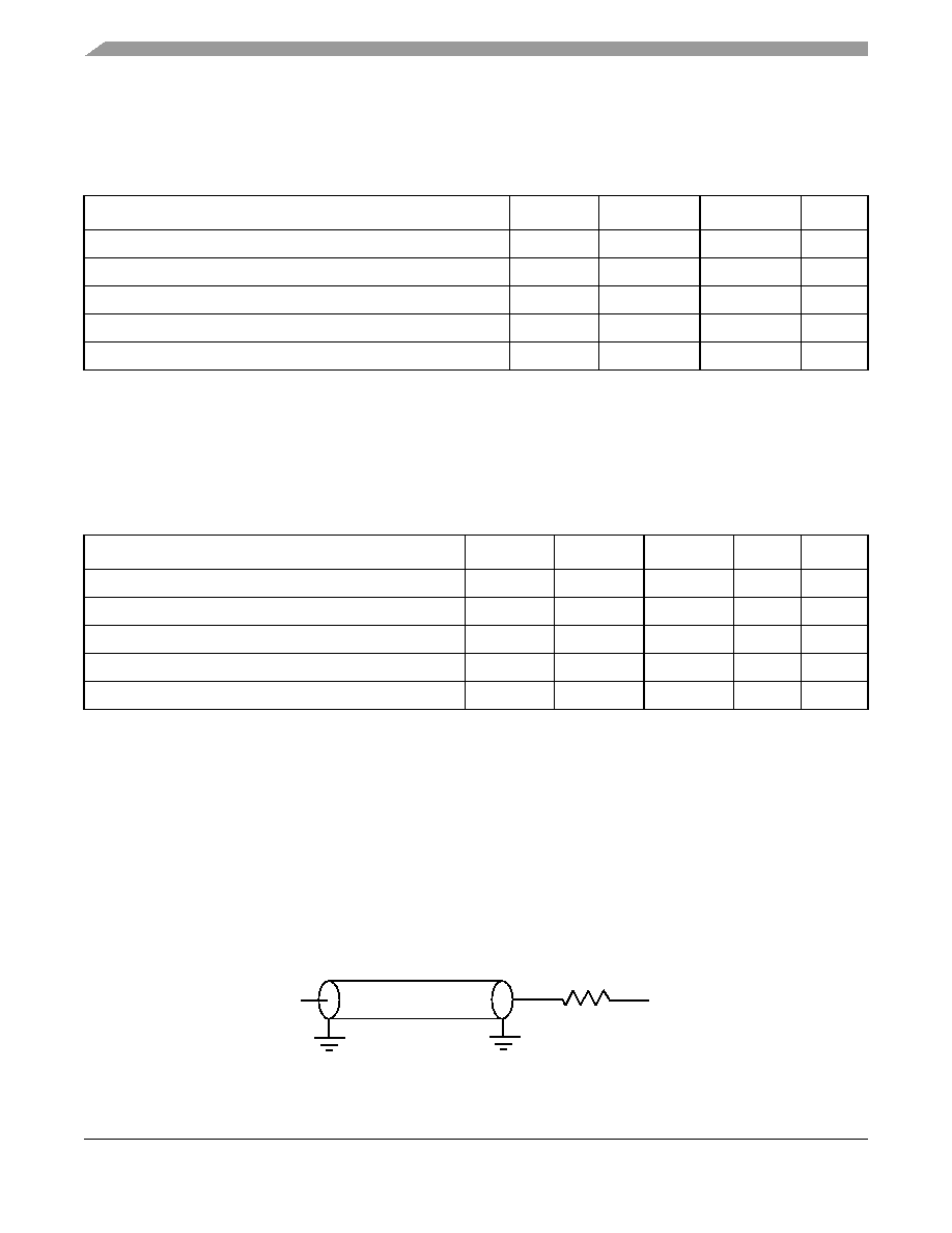
Figure 21. USB AC Test Load
Table 39. USB DC Electrical Characteristics
Parameter
Symbol
Min
Max
Unit
High-level input voltage
VIH
2
LVDD + 0.3
V
Low-level input voltage
VIL
–0.3
0.8
V
Input current
IIN
—±5
μA
High-level output voltage, IOH = –100 μAVOH
LVDD – 0.2
—
V
Low-level output voltage, IOL = 100 μAVOL
—0.2
V
Note:
Table 40. USB General Timing Parameters
Parameter
Symbol 1
Min
Max
Unit
Notes
USB clock cycle time
tUSCK
15
—
ns
1, 2
Input setup to USB clock—all inputs
tUSIVKH
4—
ns
1, 4
Input hold to USB clock—all inputs
tUSIXKH
1—
ns
1, 4
USB clock to output valid—all outputs
tUSKHOV
—9
ns
1
Output hold from USB clock—all outputs
tUSKHOX
1—
ns
1
Notes:
1. The symbols used for timing specifications follow the pattern of t(First two letters of functional block)(signal)(state)(reference)(state) for
inputs and t(First two letters of functional block)(reference)(state)(signal)(state) for outputs. For example, tUSIXKH symbolizes USB timing
(US) for the input (I) to go invalid (X) with respect to the time the USB clock reference (K) goes high (H). Also, tUSKHOX
symbolizes USB timing (US) for the us clock reference (K) to go high (H), with respect to the output (O) going invalid (X) or
output hold time.
2. All timings are in reference to USB clock.
3. All signals are measured from NVDD/2 of the rising edge of USB clock to 0.4
× NVDD of the signal in question for 3.3-V
signaling levels.
4. Input timings are measured at the pin.
5. For purposes of active/float timing measurements, the Hi-Z or off-state is defined to be when the total current delivered
through the component pin is less than or equal to the leakage current specification.
Output
Z0 = 50 Ω
NVDD/2
RL = 50 Ω
相關(guān)PDF資料 |
PDF描述 |
|---|---|
| MPC8315EVRAFDA | 32-BIT, 333 MHz, MICROPROCESSOR, PBGA620 |
| MPC8315EVRADDA | 32-BIT, 266 MHz, MICROPROCESSOR, PBGA620 |
| MPC8315EVRAGDA | 32-BIT, 400 MHz, MICROPROCESSOR, PBGA620 |
| MPC8315VRAFDA | 32-BIT, 333 MHz, MICROPROCESSOR, PBGA620 |
| MPC8321EVRAFDCA | 32-BIT, 333 MHz, RISC PROCESSOR, PBGA516 |
相關(guān)代理商/技術(shù)參數(shù) |
參數(shù)描述 |
|---|---|
| MPC8314VRADDA | 功能描述:微處理器 - MPU NON-ENCRYPT RoHS:否 制造商:Atmel 處理器系列:SAMA5D31 核心:ARM Cortex A5 數(shù)據(jù)總線寬度:32 bit 最大時鐘頻率:536 MHz 程序存儲器大小:32 KB 數(shù)據(jù) RAM 大小:128 KB 接口類型:CAN, Ethernet, LIN, SPI,TWI, UART, USB 工作電源電壓:1.8 V to 3.3 V 最大工作溫度:+ 85 C 安裝風(fēng)格:SMD/SMT 封裝 / 箱體:FBGA-324 |
| MPC8314VRAFDA | 功能描述:微處理器 - MPU NON-ENCRYPT RoHS:否 制造商:Atmel 處理器系列:SAMA5D31 核心:ARM Cortex A5 數(shù)據(jù)總線寬度:32 bit 最大時鐘頻率:536 MHz 程序存儲器大小:32 KB 數(shù)據(jù) RAM 大小:128 KB 接口類型:CAN, Ethernet, LIN, SPI,TWI, UART, USB 工作電源電壓:1.8 V to 3.3 V 最大工作溫度:+ 85 C 安裝風(fēng)格:SMD/SMT 封裝 / 箱體:FBGA-324 |
| MPC8314VRAGDA | 功能描述:微處理器 - MPU NON-ENCRYPT RoHS:否 制造商:Atmel 處理器系列:SAMA5D31 核心:ARM Cortex A5 數(shù)據(jù)總線寬度:32 bit 最大時鐘頻率:536 MHz 程序存儲器大小:32 KB 數(shù)據(jù) RAM 大小:128 KB 接口類型:CAN, Ethernet, LIN, SPI,TWI, UART, USB 工作電源電壓:1.8 V to 3.3 V 最大工作溫度:+ 85 C 安裝風(fēng)格:SMD/SMT 封裝 / 箱體:FBGA-324 |
| MPC8315 | 制造商:FREESCALE 制造商全稱:Freescale Semiconductor, Inc 功能描述:MPC8315E PowerQUICC II Pro Processor Hardware Specifications |
| MPC8315CVRADDA | 功能描述:微處理器 - MPU NON-ENCRYPT RoHS:否 制造商:Atmel 處理器系列:SAMA5D31 核心:ARM Cortex A5 數(shù)據(jù)總線寬度:32 bit 最大時鐘頻率:536 MHz 程序存儲器大小:32 KB 數(shù)據(jù) RAM 大小:128 KB 接口類型:CAN, Ethernet, LIN, SPI,TWI, UART, USB 工作電源電壓:1.8 V to 3.3 V 最大工作溫度:+ 85 C 安裝風(fēng)格:SMD/SMT 封裝 / 箱體:FBGA-324 |
發(fā)布緊急采購,3分鐘左右您將得到回復(fù)。