- 您現(xiàn)在的位置:買(mǎi)賣(mài)IC網(wǎng) > PDF目錄25624 > MQ80C32-20:RD (TEMIC SEMICONDUCTORS) 8-BIT, 20 MHz, MICROCONTROLLER, CQFP44 PDF資料下載
參數(shù)資料
| 型號(hào): | MQ80C32-20:RD |
| 廠(chǎng)商: | TEMIC SEMICONDUCTORS |
| 元件分類(lèi): | 微控制器/微處理器 |
| 英文描述: | 8-BIT, 20 MHz, MICROCONTROLLER, CQFP44 |
| 文件頁(yè)數(shù): | 22/83頁(yè) |
| 文件大?。?/td> | 8336K |
第1頁(yè)第2頁(yè)第3頁(yè)第4頁(yè)第5頁(yè)第6頁(yè)第7頁(yè)第8頁(yè)第9頁(yè)第10頁(yè)第11頁(yè)第12頁(yè)第13頁(yè)第14頁(yè)第15頁(yè)第16頁(yè)第17頁(yè)第18頁(yè)第19頁(yè)第20頁(yè)第21頁(yè)當(dāng)前第22頁(yè)第23頁(yè)第24頁(yè)第25頁(yè)第26頁(yè)第27頁(yè)第28頁(yè)第29頁(yè)第30頁(yè)第31頁(yè)第32頁(yè)第33頁(yè)第34頁(yè)第35頁(yè)第36頁(yè)第37頁(yè)第38頁(yè)第39頁(yè)第40頁(yè)第41頁(yè)第42頁(yè)第43頁(yè)第44頁(yè)第45頁(yè)第46頁(yè)第47頁(yè)第48頁(yè)第49頁(yè)第50頁(yè)第51頁(yè)第52頁(yè)第53頁(yè)第54頁(yè)第55頁(yè)第56頁(yè)第57頁(yè)第58頁(yè)第59頁(yè)第60頁(yè)第61頁(yè)第62頁(yè)第63頁(yè)第64頁(yè)第65頁(yè)第66頁(yè)第67頁(yè)第68頁(yè)第69頁(yè)第70頁(yè)第71頁(yè)第72頁(yè)第73頁(yè)第74頁(yè)第75頁(yè)第76頁(yè)第77頁(yè)第78頁(yè)第79頁(yè)第80頁(yè)第81頁(yè)第82頁(yè)第83頁(yè)

20
8021G–AVR–03/11
ATmega329P/3290P
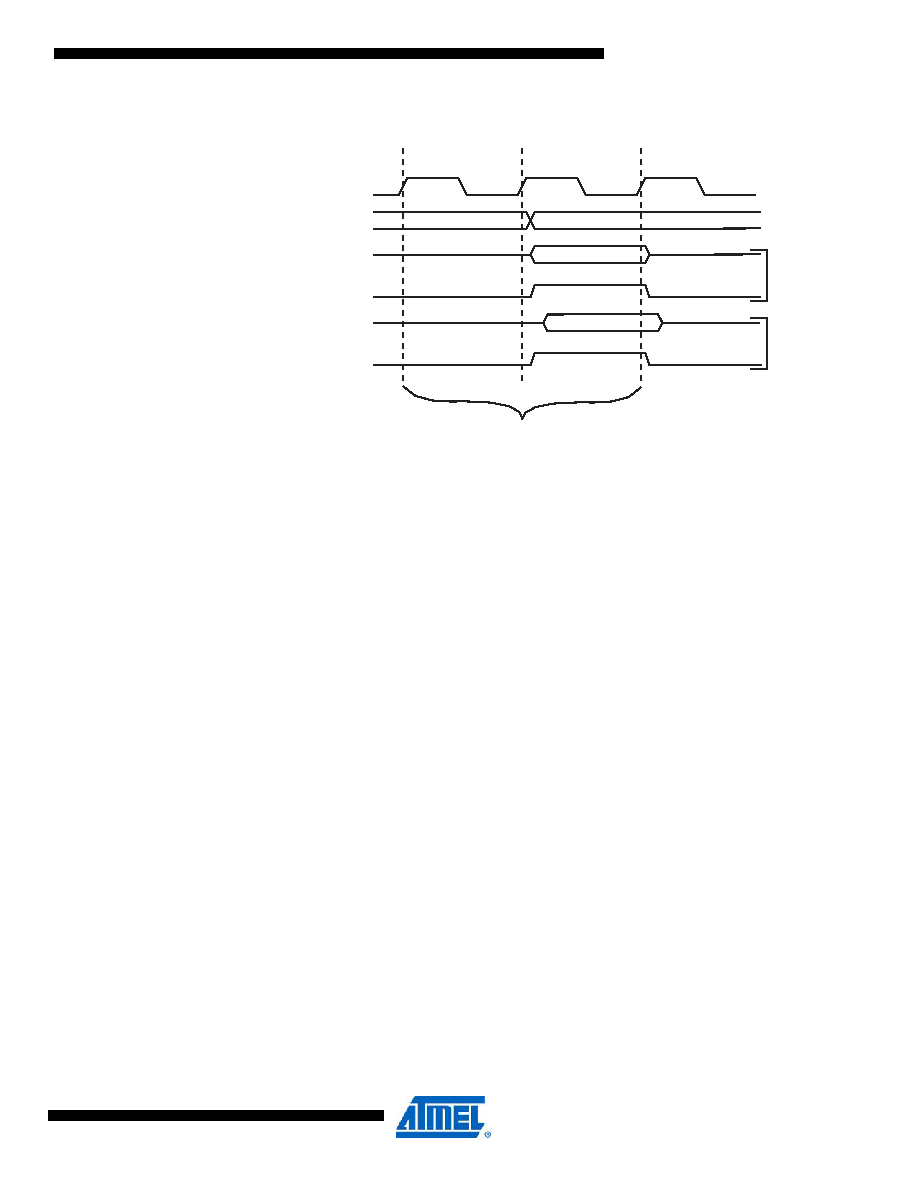
Figure 7-3.
On-chip Data SRAM Access Cycles
7.4
EEPROM Data Memory
The ATmega329P/3290P contains 1Kbytes of data EEPROM memory. It is organized as a sep-
arate data space, in which single bytes can be read and written. The EEPROM has an
endurance of at least 100,000 write/erase cycles. The access between the EEPROM and the
CPU is described in the following, specifying the EEPROM Address Registers, the EEPROM
Data Register, and the EEPROM Control Register.
For a detailed description of SPI, JTAG and Parallel data downloading to the EEPROM, see
7.4.1
EEPROM Write During Power-down Sleep Mode
When entering Power-down sleep mode while an EEPROM write operation is active, the
EEPROM write operation will continue, and will complete before the Write Access time has
passed. However, when the write operation is completed, the clock continues running, and as a
consequence, the device does not enter Power-down entirely. It is therefore recommended to
verify that the EEPROM write operation is completed before entering Power-down.
7.4.2
Preventing EEPROM Corruption
During periods of low V
CC, the EEPROM data can be corrupted because the supply voltage is
too low for the CPU and the EEPROM to operate properly. These issues are the same as for
board level systems using EEPROM, and the same design solutions should be applied.
An EEPROM data corruption can be caused by two situations when the voltage is too low. First,
a regular write sequence to the EEPROM requires a minimum voltage to operate correctly. Sec-
ondly, the CPU itself can execute instructions incorrectly, if the supply voltage is too low.
EEPROM data corruption can easily be avoided by following this design recommendation:
Keep the AVR RESET active (low) during periods of insufficient power supply voltage. This can
be done by enabling the internal Brown-out Detector (BOD). If the detection level of the internal
BOD does not match the needed detection level, an external low V
CC reset Protection circuit can
clk
WR
RD
Data
Address
Address valid
T1
T2
T3
Compute Address
Read
Wr
ite
CPU
Memory Access Instruction
Next Instruction
相關(guān)PDF資料 |
PDF描述 |
|---|---|
| MQ80C52TXXX-16SHXXX:RD | 8-BIT, MROM, 16 MHz, MICROCONTROLLER, CQFP44 |
| MC80C52TXXX-12 | 8-BIT, MROM, 12 MHz, MICROCONTROLLER, CDIP40 |
| MC88LV926DW | 88LV SERIES, PLL BASED CLOCK DRIVER, 4 TRUE OUTPUT(S), 1 INVERTED OUTPUT(S), PDSO20 |
| MC9328MX21SCVM | 32-BIT, 266 MHz, MICROPROCESSOR, PBGA289 |
| MC9S08AC16CFJE | 8-BIT, FLASH, 40 MHz, MICROCONTROLLER, PQFP32 |
相關(guān)代理商/技術(shù)參數(shù) |
參數(shù)描述 |
|---|---|
| MQ82370-20 | 制造商:Rochester Electronics LLC 功能描述:- Bulk |
| MQ8238020 | 制造商:Intel 功能描述:CONTROLLER: OTHER |
| MQ82380-20 | 制造商:Rochester Electronics LLC 功能描述:- Bulk |
| MQ82380-20/R | 制造商:Rochester Electronics LLC 功能描述: |
| MQ82592 | 制造商:Rochester Electronics LLC 功能描述:- Bulk |
發(fā)布緊急采購(gòu),3分鐘左右您將得到回復(fù)。