- 您現(xiàn)在的位置:買賣IC網(wǎng) > PDF目錄25624 > MQ80C32-20:RD (TEMIC SEMICONDUCTORS) 8-BIT, 20 MHz, MICROCONTROLLER, CQFP44 PDF資料下載
參數(shù)資料
| 型號: | MQ80C32-20:RD |
| 廠商: | TEMIC SEMICONDUCTORS |
| 元件分類: | 微控制器/微處理器 |
| 英文描述: | 8-BIT, 20 MHz, MICROCONTROLLER, CQFP44 |
| 文件頁數(shù): | 76/83頁 |
| 文件大小: | 8336K |
第1頁第2頁第3頁第4頁第5頁第6頁第7頁第8頁第9頁第10頁第11頁第12頁第13頁第14頁第15頁第16頁第17頁第18頁第19頁第20頁第21頁第22頁第23頁第24頁第25頁第26頁第27頁第28頁第29頁第30頁第31頁第32頁第33頁第34頁第35頁第36頁第37頁第38頁第39頁第40頁第41頁第42頁第43頁第44頁第45頁第46頁第47頁第48頁第49頁第50頁第51頁第52頁第53頁第54頁第55頁第56頁第57頁第58頁第59頁第60頁第61頁第62頁第63頁第64頁第65頁第66頁第67頁第68頁第69頁第70頁第71頁第72頁第73頁第74頁第75頁當(dāng)前第76頁第77頁第78頁第79頁第80頁第81頁第82頁第83頁

88
7707F–AVR–11/10
AT90USB82/162
13. Timer/Counter0 and Timer/Counter1 Prescalers
Timer/Counter0 and 1 share the same prescaler module, but the Timer/Counters can have dif-
ferent prescaler settings. The description below applies to all Timer/Counters. Tn is used as a
general name, n = 0 or 1.
13.0.1
Internal Clock Source
The Timer/Counter can be clocked directly by the system clock (by setting the CSn2:0 = 1). This
provides the fastest operation, with a maximum Timer/Counter clock frequency equal to system
clock frequency (f
CLK_I/O). Alternatively, one of four taps from the prescaler can be used as a
clock source. The prescaled clock has a frequency of either f
CLK_I/O/8, fCLK_I/O/64, fCLK_I/O/256, or
f
CLK_I/O/1024.
13.0.2
Prescaler Reset
The prescaler is free running, i.e., operates independently of the Clock Select logic of the
Timer/Counter, and it is shared by the Timer/Counter Tn. Since the prescaler is not affected by
the Timer/Counter’s clock select, the state of the prescaler will have implications for situations
where a prescaled clock is used. One example of prescaling artifacts occurs when the timer is
enabled and clocked by the prescaler (6 > CSn2:0 > 1). The number of system clock cycles from
when the timer is enabled to the first count occurs can be from 1 to N+1 system clock cycles,
where N equals the prescaler divisor (8, 64, 256, or 1024).
It is possible to use the prescaler reset for synchronizing the Timer/Counter to program execu-
tion. However, care must be taken if the other Timer/Counter that shares the same prescaler
also uses prescaling. A prescaler reset will affect the prescaler period for all Timer/Counters it is
connected to.
13.0.3
External Clock Source
An external clock source applied to the Tn pin can be used as Timer/Counter clock (clk
Tn). The
Tn pin is sampled once every system clock cycle by the pin synchronization logic. The synchro-
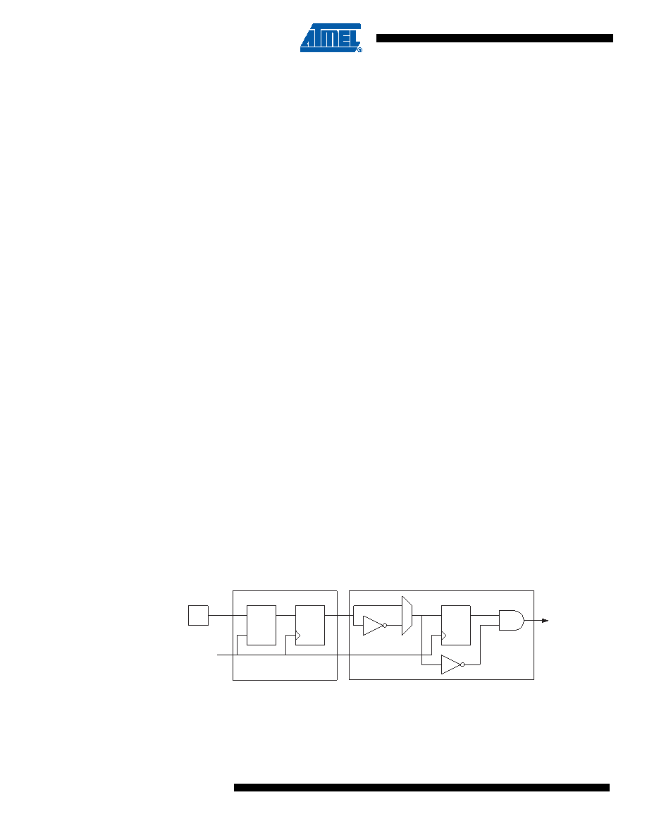
nized (sampled) signal is then passed through the edge detector. Figure 13-1 shows a functional
equivalent block diagram of the Tn synchronization and edge detector logic. The registers are
clocked at the positive edge of the internal system clock (clk
I/O). The latch is transparent in the
high period of the internal system clock.
The edge detector generates one clk
Tn pulse for each positive (CSn2:0 = 7) or negative (CSn2:0
= 6) edge it detects.
Figure 13-1. Tn/T0 Pin Sampling
The synchronization and edge detector logic introduces a delay of 2.5 to 3.5 system clock cycles
from an edge has been applied to the Tn pin to the counter is updated.
Enabling and disabling of the clock input must be done when Tn has been stable for at least one
system clock cycle, otherwise it is a risk that a false Timer/Counter clock pulse is generated.
Tn_sync
(To Clock
Select Logic)
Edge Detector
Synchronization
DQ
LE
DQ
Tn
clk
I/O
相關(guān)PDF資料 |
PDF描述 |
|---|---|
| MQ80C52TXXX-16SHXXX:RD | 8-BIT, MROM, 16 MHz, MICROCONTROLLER, CQFP44 |
| MC80C52TXXX-12 | 8-BIT, MROM, 12 MHz, MICROCONTROLLER, CDIP40 |
| MC88LV926DW | 88LV SERIES, PLL BASED CLOCK DRIVER, 4 TRUE OUTPUT(S), 1 INVERTED OUTPUT(S), PDSO20 |
| MC9328MX21SCVM | 32-BIT, 266 MHz, MICROPROCESSOR, PBGA289 |
| MC9S08AC16CFJE | 8-BIT, FLASH, 40 MHz, MICROCONTROLLER, PQFP32 |
相關(guān)代理商/技術(shù)參數(shù) |
參數(shù)描述 |
|---|---|
| MQ82370-20 | 制造商:Rochester Electronics LLC 功能描述:- Bulk |
| MQ8238020 | 制造商:Intel 功能描述:CONTROLLER: OTHER |
| MQ82380-20 | 制造商:Rochester Electronics LLC 功能描述:- Bulk |
| MQ82380-20/R | 制造商:Rochester Electronics LLC 功能描述: |
| MQ82592 | 制造商:Rochester Electronics LLC 功能描述:- Bulk |
發(fā)布緊急采購,3分鐘左右您將得到回復(fù)。