- 您現(xiàn)在的位置:買賣IC網(wǎng) > PDF目錄383644 > MT9043 (Mitel Networks Corporation) T1/E1 System Synchronizer(T1/E1 系統(tǒng)同步裝置(由一個數(shù)字鎖相環(huán)組成)) PDF資料下載
參數(shù)資料
| 型號: | MT9043 |
| 廠商: | Mitel Networks Corporation |
| 英文描述: | T1/E1 System Synchronizer(T1/E1 系統(tǒng)同步裝置(由一個數(shù)字鎖相環(huán)組成)) |
| 中文描述: | T1/E1的系統(tǒng)同步(T1/E1的系統(tǒng)同步裝置(由一個數(shù)字鎖相環(huán)組成)) |
| 文件頁數(shù): | 5/24頁 |
| 文件大?。?/td> | 100K |
| 代理商: | MT9043 |
Advance Information
MT9043
5
During a switch from one reference to the other, the
State Machine first changes the mode of the device
from Normal to Freerun. The Compare Circuit then
measures the phase delay between the current
phase (feedback signal) and the phase of the new
reference signal. This delay value is passed to the
Programmable Delay Circuit (See Figure 3). The
state machine then returns the device to Normal
Mode and the DPLL begins using the new virtual
reference signal. The difference between the phase
position of the new virtual reference and the previous
reference is less than 1
μ
s.
Since internal delay circuitry maintains the alignment
between the old virtual reference and the new virtual
reference, a phase error may exist between the
selected input reference signal and the output signal
of the DPLL. This phase error is a function of the
difference in phase between the two input reference
signals during reference rearrangements. Each time
a reference switch is made, the delay between input
signal and output signal will change. The value of
this delay is the accumulation of the error measured
during each reference switch.
The programmable delay circuit can be zeroed by
applying a logic low pulse to the TIE Circuit Reset
(TCLR) pin. A minimum reset pulse width is 300ns.
This results in a phase alignment between the input
reference signal and the output signal as shown in
Figure 12. The speed of the phase alignment
correction
is
limited
to
convergence is in the direction of least phase travel.
5ns
per
125us,
and
The state diagram of Figure 7 indicates the state
changes during which the TIE corrector circuit is
activated.
Digital Phase Lock Loop (DPLL)
As shown in Figure 4, the DPLL of the MT9043
consists of a Phase Detector, Limiter, Loop Filter,
Digitally Controlled Oscillator, and a Control Circuit.
Phase Detector
- the Phase Detector compares the
virtual reference signal from the TIE Corrector circuit
with the feedback signal from the Frequency Select
MUX
circuit,
and
provides
corresponding to the phase difference between the
two. This error signal is passed to the Limiter circuit.
The Frequency Select MUX allows the proper
feedback signal to be externally selected (e.g., 8kHz,
1.544MHz, 2.048MHz or 19.44MHz).
an
error
signal
Limiter
- the Limiter receives the error signal from
the Phase Detector and ensures that the DPLL
responds to all input transient conditions with a
maximum output phase slope of 5ns per 125us. This
is well within the maximum phase slope of 7.6ns per
125us or 81ns per 1.326ms specified by AT&T
TR62411
and
Bellcore
respectively.
GR-1244-CORE,
Loop Filter
- the Loop Filter is similar to a first order
low pass filter with a 1.9 Hz cutoff frequency for all
four
reference
frequency
1.544MHz, 2.048MHz or 19.44MHz). This filter
ensures that the jitter transfer requirements in ETS
300 011 and AT&T TR62411 are met.
selections
(8kHz,
Control Circuit
- the Control Circuit uses status and
control information from the State Machine and the
Input Impairment Circuit to set the mode of the
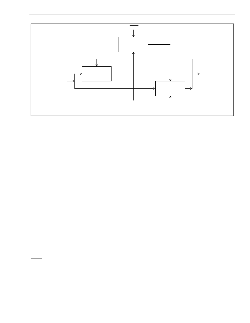
Figure 3 - TIE Corrector Circuit
Programmable
Delay Circuit
Control Signal
Delay Value
TCLR
Resets Delay
Compare
Circuit
TIE Corrector
Enable
from
State Machine
Control
Circuit
Feedback
Signal from
Frequency
Select MUX
PRI or SEC
from
Reference
Select Mux
Virtual
Reference
to DPLL
相關(guān)PDF資料 |
PDF描述 |
|---|---|
| MT9044 | T1/E1/OC3 System Synchronizer(T1/E1/OC3 系統(tǒng)同步裝置(由一個數(shù)字鎖相環(huán)組成)) |
| MT90500 | Multi-Channel ATM AAL1 SAR(多通道 ATM AAL1分段及重組設(shè)備(基于通訊總線的系統(tǒng)與ATM網(wǎng)絡(luò)的接口)) |
| MT90500 | Multi-Channel ATM AAL1 SAR |
| MT90500AL | Multi-Channel ATM AAL1 SAR |
| MT90502 | Multi-Channel AAL2 SAR(多通道 ATM AAL2分段及重組設(shè)備(基于通訊總線的系統(tǒng)與ATM網(wǎng)絡(luò)的接口)) |
相關(guān)代理商/技術(shù)參數(shù) |
參數(shù)描述 |
|---|---|
| MT9043AN | 制造商:Microsemi Corporation 功能描述: |
| MT9043AN1 | 制造商:Microsemi Corporation 功能描述:PB FREE T1/E1 SYSTEM SYNCHRONIZER 制造商:Microsemi Corporation 功能描述:FRAMER E1/T1 3.3V 48SSOP - Rail/Tube 制造商:MICROSEMI CONSUMER MEDICAL PRODUCT GROUP 功能描述:IC SYNCHRONIZER T1/E1 48SSOP 制造商:Microsemi Corporation 功能描述:IC SYNCHRONIZER T1/E1 48SSOP |
| MT9043AN48PINSSOP | 制造商:ZARLINK 制造商全稱:Zarlink Semiconductor Inc 功能描述:T1/E1 System Synchronizer |
| MT9043ANR1 | 制造商:Microsemi Corporation 功能描述:FRAMER E1 /T1 3.3V 48SSOP - Tape and Reel 制造商:MICROSEMI CONSUMER MEDICAL PRODUCT GROUP 功能描述:IC SYNCHRONIZER T1/E1 48SSOP 制造商:Microsemi Corporation 功能描述:IC SYNCHRONIZER T1/E1 48SSOP |
| MT9044 | 制造商:MITEL 制造商全稱:Mitel Networks Corporation 功能描述:T1/E1/OC3 System Synchronizer |
發(fā)布緊急采購,3分鐘左右您將得到回復(fù)。