- 您現(xiàn)在的位置:買賣IC網(wǎng) > PDF目錄383644 > MT90732AP (Mitel Networks Corporation) Ultraframer DS3/E3/DS2/E2/DS1/E1/DS0 PDF資料下載
參數(shù)資料
| 型號(hào): | MT90732AP |
| 廠商: | Mitel Networks Corporation |
| 元件分類: | 通信及網(wǎng)絡(luò) |
| 英文描述: | Ultraframer DS3/E3/DS2/E2/DS1/E1/DS0 |
| 中文描述: | Ultraframer DS3/E3/DS2/E2/DS1/E1/DS0 |
| 文件頁(yè)數(shù): | 3/8頁(yè) |
| 文件大?。?/td> | 61K |
| 代理商: | MT90732AP |
Advance Information
CMOS
MT90732
5-17
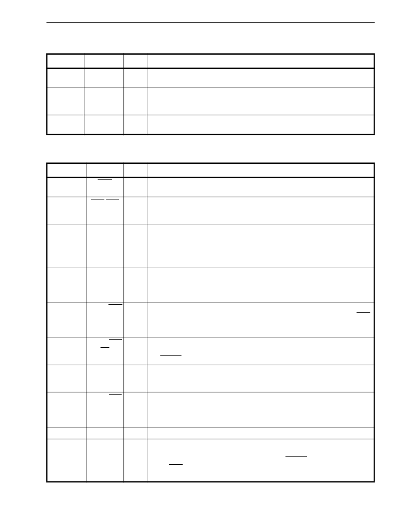
Note: I = Input; O = Output; P = Power
Line Side Transmit
Pin #
Name
I/O/P
Description
31
TP/TDL
O
Transmit Positive Rail/Transmit NRZ Data.
Transmit positive rail/NRZ data
sent out of E2/E3 Framer.
32
TCK/TCKL
O
Transmit Clock Rail/Transmit Clock NRZ.
The transmit clock is used for
clocking out the dual rail/NRZ data signals. The TCK/TCKL clock signal is
derived from the XCK clock.
33
TN
O
Transmit Negative Rail Data.
Transmit negative rail data sent out of E2/E3
Framer.
Terminal Interface
Pin #
Name
I/O/P
Description
61
RCG
O
Receive Clock Gapped.
An active low signal indicates the receive framing
and service bit locations in the serial mode only.
62
RNF/RSF
O
Receive Framing Pulse.
Framing pulse is synchronous with the last nibble for
the nibble-parallel interface, and with the first bit in the frame for the bit-serial
interface.
63
RNIB3/RSD
O
Receive Nibble Bit 3/Receive Serial Data.
Bit 3 is the most significant bit in
the nibble and corresponds to the first bit received in the nibble. The framing
pattern, service bits, and BIP-4 nibble are not provided as parallel data. In the
serial mode receive data signal consists of all bits, including the framing pat-
tern and service bits.
64
RNIB2/TDO
UT
O
Receive Nibble Bit 2/Transmit Reference Generator Data Output.
In the
nibble-parallel mode, it is Bit 2 of the received nibble.The reference generator
is enabled in the serial mode. The output data signal (TDOUT) consists of all
ones in place of the framing bits and zeros elsewhere in the frame.
65
RNIB1/TCG
O
Receive Nibble Bit 1/Transmit Reference Generator Clock Gap Signal.
In
the nibble-parallel mode, it is Bit 1 of the received nibble. The active low TCG
signal indicates the location of the framing pattern and the service bits in the
frame.
66
RNIB0/TFO
UT
O
Receive Nibble Bit 0/Transmit Reference Generator Framing Pulse.
Bit 0
is the least significant bit in the nibble and is the last bit received. The active
low TFOUT signal is synchronous with the first bit in the frame.
67
RNC/RSC
O
Receive Nibble Clock/Receive Serial Clock.
The nibble and serial clocks are
derived from the line side dual rail/NRZ clock signal (RCK/RCKL). RNC is
gapped during framing pattern, service bit and BIP-4 bit times.
53
XNIB3/XSF
I
Transmit Nibble Bit 3/Transmit Serial Framing Pulse.
In the nibble-parallel
mode, bit 3 is the most significant bit in the nibble and corresponds to the first
bit transmitted in the nibble. When the terminal interface is serial, the negative
framing pulse is synchronous with the first bit in the frame.
54
XNIB2
I
Transmit Nibble Bit 2.
Bit 2 in the 4-bit nibble.
55
XNIB1/TCI
N
I
Transmit Nibble Bit 1/Transmit Reference Generator Clock In.
Bit 1 in the
transmit nibble. For a serial interface, the TCIN is used to derive the clock out
(TCOUT), data signal (TDOUT), framing pulse (TFOUT), and gapped clock
signal (TCG).The reference generator signals are provided for multiplexing the
external payload data into the serial frame.
相關(guān)PDF資料 |
PDF描述 |
|---|---|
| MT90732 | Ultraframer DS3/E3/DS2/E2/DS1/E1/DS0 |
| MT90733 | Ultraframer DS3/E3/DS2/E2/DS1/E1/DS0 |
| MT90733AP | Ultraframer DS3/E3/DS2/E2/DS1/E1/DS0 |
| MT9074 | T1/E1/J1 Single Chip Transceiver |
| MT9074AL | T1/E1/J1 Single Chip Transceiver |
相關(guān)代理商/技術(shù)參數(shù) |
參數(shù)描述 |
|---|---|
| MT90733 | 制造商:MITEL 制造商全稱:Mitel Networks Corporation 功能描述:CMOS DS3 Framer (DS3F) |
| MT90733AP | 制造商:MITEL 制造商全稱:Mitel Networks Corporation 功能描述:CMOS DS3 Framer (DS3F) |
| MT9074 | 制造商:ZARLINK 制造商全稱:Zarlink Semiconductor Inc 功能描述:T1/E1/J1 Single Chip Transceiver |
| MT9074_05 | 制造商:ZARLINK 制造商全稱:Zarlink Semiconductor Inc 功能描述:T1/E1/J1 Single Chip Transceiver |
| MT9074AL | 制造商:Microsemi Corporation 功能描述:FRAMER E1/J1/T1 5V 100MQFP - Trays 制造商:Zarlink Semiconductor Inc 功能描述:FRAMER E1/J1/T1 5V 100MQFP - Trays |
發(fā)布緊急采購(gòu),3分鐘左右您將得到回復(fù)。