- 您現(xiàn)在的位置:買賣IC網(wǎng) > PDF目錄68018 > MTA81010T-XT/SO 8-BIT, OTPROM, 4 MHz, RISC MICROCONTROLLER, PDSO28 PDF資料下載
參數(shù)資料
| 型號: | MTA81010T-XT/SO |
| 元件分類: | 微控制器/微處理器 |
| 英文描述: | 8-BIT, OTPROM, 4 MHz, RISC MICROCONTROLLER, PDSO28 |
| 封裝: | 0.300 INCH, SOIC-28 |
| 文件頁數(shù): | 35/76頁 |
| 文件大小: | 745K |
| 代理商: | MTA81010T-XT/SO |
第1頁第2頁第3頁第4頁第5頁第6頁第7頁第8頁第9頁第10頁第11頁第12頁第13頁第14頁第15頁第16頁第17頁第18頁第19頁第20頁第21頁第22頁第23頁第24頁第25頁第26頁第27頁第28頁第29頁第30頁第31頁第32頁第33頁第34頁當(dāng)前第35頁第36頁第37頁第38頁第39頁第40頁第41頁第42頁第43頁第44頁第45頁第46頁第47頁第48頁第49頁第50頁第51頁第52頁第53頁第54頁第55頁第56頁第57頁第58頁第59頁第60頁第61頁第62頁第63頁第64頁第65頁第66頁第67頁第68頁第69頁第70頁第71頁第72頁第73頁第74頁第75頁第76頁
MTA81010
DS39005D-page 40
1995 Microchip Technology Inc.
15.0
ELECTRICAL CHARACTERISTICS
15.1
Absolute Maximum Ratings*
Ambient temperature under bias .............................................................................................................-55
°C to +125°C
Storage Temperature.............................................................................................................................. -65
°C to +150°C
Voltage on VDD with respect to VSS ................................................................................................................ 0 to +7.5V
Voltage on MCLR with respect to VSS................................................................................................................0 to +14V
Voltage on all other pins with respect to VSS .................................................................................. -0.6V to (VDD + 0.6V)
Total power Dissipation (Note 1) ..........................................................................................................................800 mW
Maximum Current out of VSS pin...........................................................................................................................150 mA
Maximum Current into VDD pin................................................................................................................................50 mA
Maximum Current into an input pin (T0CKI only)
...........................................................................................................± 500 A
Input clamp current, IIK (VI < 0 or VI > VDD)
.................................................................................................................... ± 20 mA
Output clamp current, IOK (V0 < 0 or V0 > VDD)
............................................................................................................. ± 20 mA
Maximum Output Current sunk by any I/O pin ........................................................................................................25 mA
Maximum Output Current sourced by any I/O pin ...................................................................................................20 mA
Maximum Output Current sourced by a single I/O port (PortA, B or C) ..................................................................40 mA
Maximum Output Current sunk by a single I/O port (PortA, B or C)........................................................................50 mA
Note 1: Total power dissipation should not exceed 800 mW for the package. Power dissipation is calculated as
follows: Pdis = VDD x {IDD -
∑ IOH} + ∑ {(VDD-VOH) x IOH} + ∑(VOL x IOL)
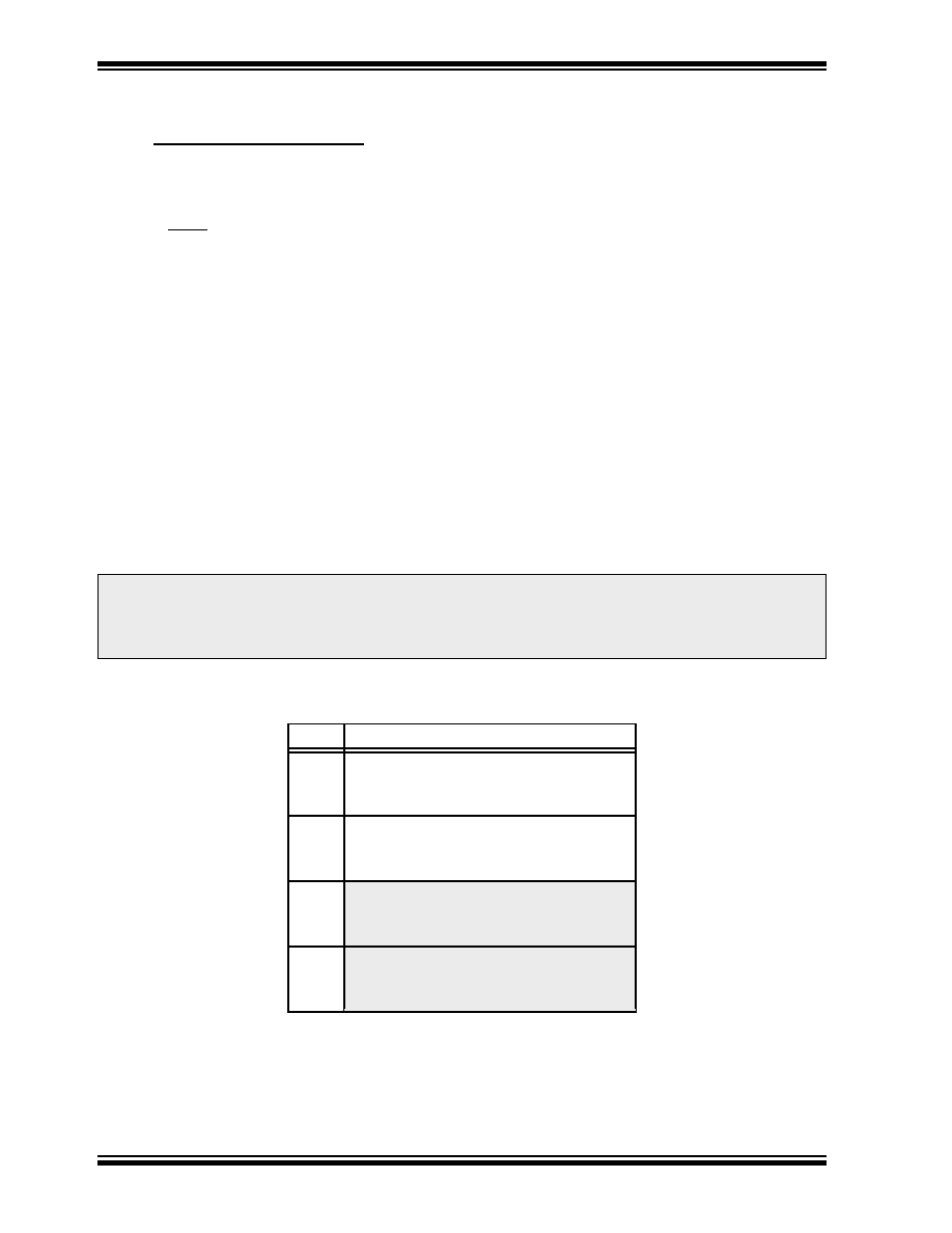
TABLE 15-1:
CROSS REFERENCE OF DEVICE SPECS FOR OSCILLATOR CONFIGURATIONS
AND FREQUENCIES OF OPERATION (COMMERCIAL DEVICES)
* Notice:
Stresses above those listed under “Maximum Ratings” may cause permanent damage to the device.
This is a stress rating only and functional operation of the device at those or any other conditions above
those indicated in the operation listings of this specification is not implied. Exposure to maximum rating
conditions for extended periods may affect device reliability.
OSC
PIC16C5X-04
RC
VDD: 3.0V to 6.25V
IDD:
2.4 mA Max. at 5.5V
IPD:
4
A Max. at 3.0V WDT dis
Freq: 4 MHz Max.
XT
VDD: 3.0V to 6.25V
IDD:
2.4 mA Max. at 5.5V
IPD:
5
A Max. at 3.0V WDT dis
Freq: 4 MHz Max.
HS
VDD: 4.5V to 5.5V
IDD:
1.8 mA typ. at 5.5V
IPD:0.3
A typ. at 3.0V WDT dis
Freq: 4 MHz Max.
LP
VDD: 4.5V to 5.5V
IDD:17
A typ. at 32 kHz, 3.0V
IPD:0.3
A typ. at 3.0V WDT dis
Freq: 200 kHz typ.
Note:
The shaded sections indicate oscillator
selections which are tested for functionality,
but not for MIN/MAX specifications. It is
recommended that the user select the
device
type
that
guarantees
the
specifications required.
相關(guān)PDF資料 |
PDF描述 |
|---|---|
| MTA81010S-XTI/SO | 8-BIT, OTPROM, 4 MHz, RISC MICROCONTROLLER, PDSO28 |
| MTA81010-LPI/SO | 8-BIT, OTPROM, 4 MHz, RISC MICROCONTROLLER, PDSO28 |
| MTA85402-20/SS | 8-BIT, OTPROM, 20 MHz, RISC MICROCONTROLLER, PDSO20 |
| MTA85812-04E/SS | 8-BIT, OTPROM, 4 MHz, RISC MICROCONTROLLER, PDSO20 |
| MTA85802-10E/SS | 8-BIT, OTPROM, 10 MHz, RISC MICROCONTROLLER, PDSO20 |
相關(guān)代理商/技術(shù)參數(shù) |
參數(shù)描述 |
|---|---|
| MTA8106DGVRA | 功能描述:SW TOGGLE SPDT VERT RT ANG PC 6A RoHS:否 類別:開關(guān) >> 撥動開關(guān) 系列:MTA 綠 標(biāo)準(zhǔn)包裝:1 系列:A 電路:雙刀雙擲 開關(guān)功能:開-開-開 觸點(diǎn)額定電壓:6A @ 125VAC 觸動器類型:扁平型 觸動器長度:11.38mm 發(fā)光:不發(fā)光 安裝類型:面板安裝 端接類型:焊片 軸襯螺紋:1/4-40 包裝:散裝 |
| MTA8106DVRA | 功能描述:SWITCH TOGGLE SPDT VRA PC 6A RoHS:否 類別:開關(guān) >> 撥動開關(guān) 系列:MTA 綠 標(biāo)準(zhǔn)包裝:1 系列:A 電路:雙刀雙擲 開關(guān)功能:開-開-開 觸點(diǎn)額定電壓:6A @ 125VAC 觸動器類型:扁平型 觸動器長度:11.38mm 發(fā)光:不發(fā)光 安裝類型:面板安裝 端接類型:焊片 軸襯螺紋:1/4-40 包裝:散裝 |
| MTA8106DVRA04 | 功能描述:SWITCH TOGGLE SPDT VRA PC 6A RoHS:是 類別:開關(guān) >> 撥動開關(guān) 系列:MTA 綠 標(biāo)準(zhǔn)包裝:1 系列:A 電路:雙刀雙擲 開關(guān)功能:開-開-開 觸點(diǎn)額定電壓:6A @ 125VAC 觸動器類型:扁平型 觸動器長度:11.38mm 發(fā)光:不發(fā)光 安裝類型:面板安裝 端接類型:焊片 軸襯螺紋:1/4-40 包裝:散裝 |
| MTA8106EGRA | 功能描述:SW TOGGLE SPDT RT ANG PC 6A RoHS:否 類別:開關(guān) >> 撥動開關(guān) 系列:MTA 綠 標(biāo)準(zhǔn)包裝:1 系列:A 電路:雙刀雙擲 開關(guān)功能:開-開-開 觸點(diǎn)額定電壓:6A @ 125VAC 觸動器類型:扁平型 觸動器長度:11.38mm 發(fā)光:不發(fā)光 安裝類型:面板安裝 端接類型:焊片 軸襯螺紋:1/4-40 包裝:散裝 |
| MTA8106EGRA04 | 功能描述:SWITCH TOGGLE SPDT RT ANG PC 6A RoHS:是 類別:開關(guān) >> 撥動開關(guān) 系列:MTA 綠 標(biāo)準(zhǔn)包裝:1 系列:A 電路:雙刀雙擲 開關(guān)功能:開-開-開 觸點(diǎn)額定電壓:6A @ 125VAC 觸動器類型:扁平型 觸動器長度:11.38mm 發(fā)光:不發(fā)光 安裝類型:面板安裝 端接類型:焊片 軸襯螺紋:1/4-40 包裝:散裝 |
發(fā)布緊急采購,3分鐘左右您將得到回復(fù)。