- 您現(xiàn)在的位置:買賣IC網(wǎng) > PDF目錄11733 > ORSO82G5-2FN680I (Lattice Semiconductor Corporation)IC TRANCEIVERS FPSC 680FPBGA PDF資料下載
參數(shù)資料
| 型號(hào): | ORSO82G5-2FN680I |
| 廠商: | Lattice Semiconductor Corporation |
| 文件頁數(shù): | 91/153頁 |
| 文件大小: | 0K |
| 描述: | IC TRANCEIVERS FPSC 680FPBGA |
| 產(chǎn)品變化通告: | Product Discontinuation 01/Aug/2011 |
| 標(biāo)準(zhǔn)包裝: | 24 |
| 系列: | * |
第1頁第2頁第3頁第4頁第5頁第6頁第7頁第8頁第9頁第10頁第11頁第12頁第13頁第14頁第15頁第16頁第17頁第18頁第19頁第20頁第21頁第22頁第23頁第24頁第25頁第26頁第27頁第28頁第29頁第30頁第31頁第32頁第33頁第34頁第35頁第36頁第37頁第38頁第39頁第40頁第41頁第42頁第43頁第44頁第45頁第46頁第47頁第48頁第49頁第50頁第51頁第52頁第53頁第54頁第55頁第56頁第57頁第58頁第59頁第60頁第61頁第62頁第63頁第64頁第65頁第66頁第67頁第68頁第69頁第70頁第71頁第72頁第73頁第74頁第75頁第76頁第77頁第78頁第79頁第80頁第81頁第82頁第83頁第84頁第85頁第86頁第87頁第88頁第89頁第90頁當(dāng)前第91頁第92頁第93頁第94頁第95頁第96頁第97頁第98頁第99頁第100頁第101頁第102頁第103頁第104頁第105頁第106頁第107頁第108頁第109頁第110頁第111頁第112頁第113頁第114頁第115頁第116頁第117頁第118頁第119頁第120頁第121頁第122頁第123頁第124頁第125頁第126頁第127頁第128頁第129頁第130頁第131頁第132頁第133頁第134頁第135頁第136頁第137頁第138頁第139頁第140頁第141頁第142頁第143頁第144頁第145頁第146頁第147頁第148頁第149頁第150頁第151頁第152頁第153頁
Lattice Semiconductor
ORCA ORSO42G5 and ORSO82G5 Data Sheet
42
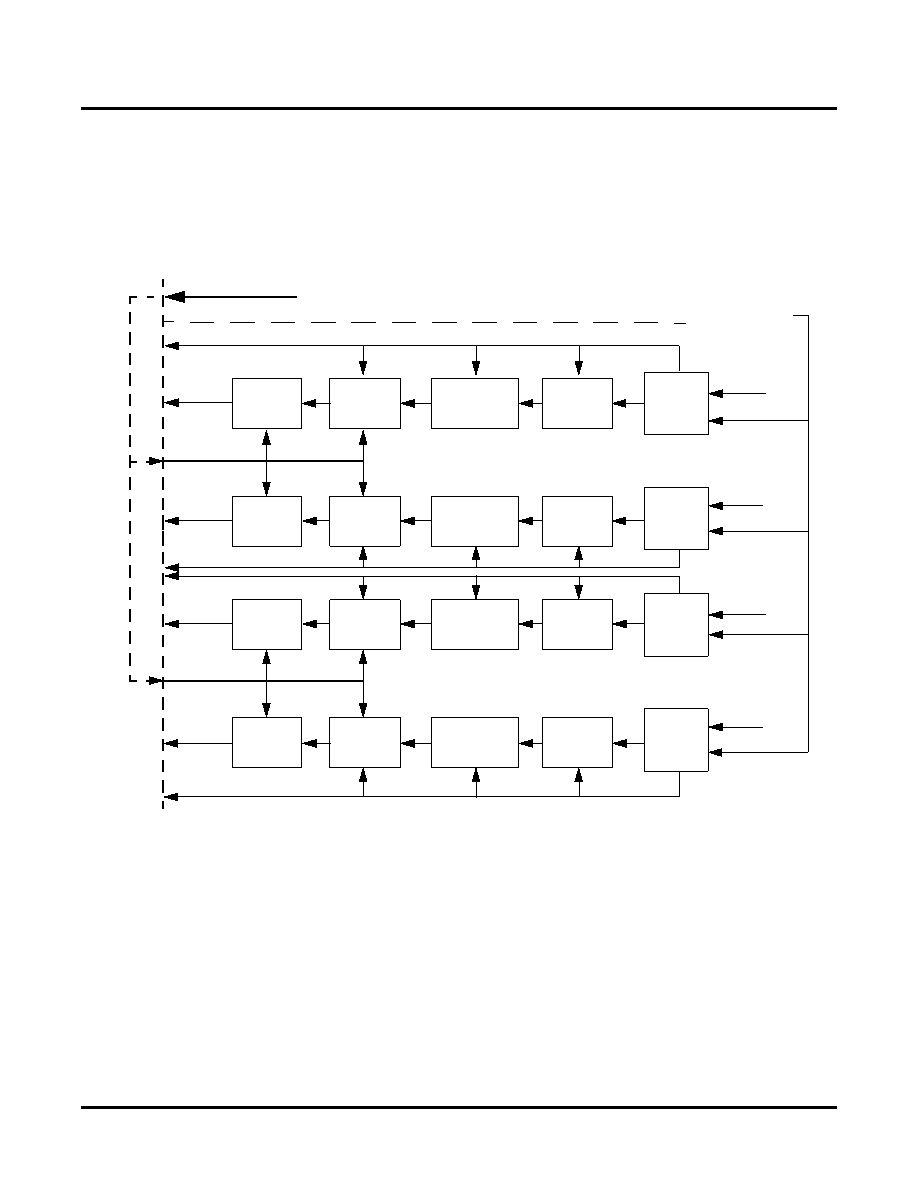
SONET Mode Block Alignment – ORSO82G5
Figure 28 describes the clocks and recommended clocking for block alignment in the SONET mode. For block
alignment, the low speed portion for each block should be sourced by a single clock. As the gure shows, for block
A, RSYSCLKA1 and RSYSCLKA2 should be sourced by RCK78A. For block B, RSYSCLKB1 and RSYSCLKB2
should be sourced by RCLK78B. RCLK78A can be sourced by any channel in block A and RCLK78B can be
sourced by any channel in block B.
Figure 28. Receive Clocking Diagram for Four-Channel Alignment in Block A – ORSO82G5
SONET Mode Octal Alignment – ORSO82G5
Figure 29 shows the clocking scheme for eight-channel alignment. In this application, all four clocks RSYSCLKA1,
RSYSCLKA2, RSYSCLKB1 and RSYSCLKB2 should be sourced from a common clock. Either RCK78A or
RCK78B can be used as a common clock source. The gure shows RCK78A being used as the clock source.
FPGA
RCK78A
SPE
Generator
SPE
Generator
SPE
Generator
SPE
Generator
Alignment
FIFO
Alignment
FIFO
Alignment
FIFO
Alignment
FIFO
Framer,
Descrambler
Framer,
Descrambler
Framer,
Descrambler
Framer,
Descrambler
DEMUX
RSYSCLKA1
Logic Common to Block
REFCLKA[P,N]
(155.52 MHz)
Channel AA
Channel AB
HDIN[P:N]_AA
2.488 Gbits/s
HDIN[P:N]_AB
2.488 Gbits/s
RSYSCLKA2
Channel AC
Channel AD
RWCKAD
RWCKAA
HDIN[P:N]_AA
2.488 Gbits/s
HDIN[P:N]_AB
2.488 Gbits/s
SERDES
DEMUX
SERDES
DEMUX
SERDES
DEMUX
SERDES
相關(guān)PDF資料 |
PDF描述 |
|---|---|
| PIC12CE519/JW | IC MCU EPROM 1KX12 W/EE 8CDIP |
| PIC32MX460F512L-80V/PT | IC MCU 32BIT 512KB FLASH 100TQFP |
| PIC32MX575F512H-80V/MR | IC MCU 32BIT 512KB FLASH 64QFN |
| VI-J4D-IW-F4 | CONVERTER MOD DC/DC 85V 100W |
| PIC32MX775F256H-80V/MR | IC MCU 32BIT 256KB FLASH 64QFN |
相關(guān)代理商/技術(shù)參數(shù) |
參數(shù)描述 |
|---|---|
| ORSO82G5-2FN680I1 | 功能描述:FPGA - 現(xiàn)場可編程門陣列 10368 LUT 372 I/O RoHS:否 制造商:Altera Corporation 系列:Cyclone V E 柵極數(shù)量: 邏輯塊數(shù)量:943 內(nèi)嵌式塊RAM - EBR:1956 kbit 輸入/輸出端數(shù)量:128 最大工作頻率:800 MHz 工作電源電壓:1.1 V 最大工作溫度:+ 70 C 安裝風(fēng)格:SMD/SMT 封裝 / 箱體:FBGA-256 |
| ORSO82G5-3BM680C | 功能描述:FPGA - 現(xiàn)場可編程門陣列 10368 LUT 372 I/O RoHS:否 制造商:Altera Corporation 系列:Cyclone V E 柵極數(shù)量: 邏輯塊數(shù)量:943 內(nèi)嵌式塊RAM - EBR:1956 kbit 輸入/輸出端數(shù)量:128 最大工作頻率:800 MHz 工作電源電壓:1.1 V 最大工作溫度:+ 70 C 安裝風(fēng)格:SMD/SMT 封裝 / 箱體:FBGA-256 |
| ORSO82G5-3F680C | 功能描述:FPGA - 現(xiàn)場可編程門陣列 ORCA FPSC 2.7GBITS/s BP XCVR 643K RoHS:否 制造商:Altera Corporation 系列:Cyclone V E 柵極數(shù)量: 邏輯塊數(shù)量:943 內(nèi)嵌式塊RAM - EBR:1956 kbit 輸入/輸出端數(shù)量:128 最大工作頻率:800 MHz 工作電源電壓:1.1 V 最大工作溫度:+ 70 C 安裝風(fēng)格:SMD/SMT 封裝 / 箱體:FBGA-256 |
| ORSO82G5-3FN680C | 功能描述:FPGA - 現(xiàn)場可編程門陣列 ORCA FPSC 1.5V 2.7 G b Bpln Xcvr 643K Gt RoHS:否 制造商:Altera Corporation 系列:Cyclone V E 柵極數(shù)量: 邏輯塊數(shù)量:943 內(nèi)嵌式塊RAM - EBR:1956 kbit 輸入/輸出端數(shù)量:128 最大工作頻率:800 MHz 工作電源電壓:1.1 V 最大工作溫度:+ 70 C 安裝風(fēng)格:SMD/SMT 封裝 / 箱體:FBGA-256 |
| ORSO82G5-3FN680C1 | 功能描述:FPGA - 現(xiàn)場可編程門陣列 10368 LUT 372 I/O RoHS:否 制造商:Altera Corporation 系列:Cyclone V E 柵極數(shù)量: 邏輯塊數(shù)量:943 內(nèi)嵌式塊RAM - EBR:1956 kbit 輸入/輸出端數(shù)量:128 最大工作頻率:800 MHz 工作電源電壓:1.1 V 最大工作溫度:+ 70 C 安裝風(fēng)格:SMD/SMT 封裝 / 箱體:FBGA-256 |
發(fā)布緊急采購,3分鐘左右您將得到回復(fù)。